
Datasheet


7
LTC3736-1
37361f
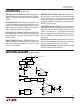
FU CTIO AL DIAGRA
U
U
W
–
+
–
+
–
+
SHDN
0.6V
V
REF
EXTSS
0.7µA
CLK1
CLK2
0.54V
V
FB1
V
FB2
SLOPE1
SLOPE2
RUN/SS
V
IN
C
VIN
V
IN
(TO CONTROLLER 1, 2)
R
VIN
SSDIS
FREQ
UNDERVOLTAGE
LOCKOUT
SPREAD
SPECTRUM
OSCILLATOR
SLOPE
COMP
VOLTAGE
REFERENCE
t
SEC
= 1ms
INTSS
IPROG1
IPROG2
IPRG1
IPRG2
VOLTAGE
CONTROLLED
OSCILLATOR
MAXIMUM
SENSE VOLTAGE
SELECT
PGOOD
SHDN
OV1
UV1
UV2
OV2
37361 FD
(Common Circuitry)
TG1/TG2 (Pins 17, 15/Pins 20, 18): Top (PMOS) Gate Drive
Output. These pins drive the gates of the external P-channel
MOSFETs. These pins have an output swing from PGND to
SENSE
+
.
SSDIS (Pin 18/Pin 21): Spread Spectrum Disable Input. Tie
this pin to V
IN
to disable spread spectrum operation. In this
mode, the LTC3736-1 operates at a constant frequency
determined by the voltage on the FREQ pin. Tie this pin to
GND to enable spread spectrum operation.
BG1/BG2 (Pins 19, 13/Pins 22, 16): Bottom (NMOS) Gate
Drive Output. These pins drive the gates of the external N-
channel MOSFETs. These pins have an output swing from
PGND to SENSE
+
.
SENSE1
+
/SENSE2
+
(Pins 21, 11/Pins 24, 14): Positive
Input to Differential Current Comparator. Also powers the
gate drivers. Normally connected to the source of the ex-
ternal P-channel MOSFET.
SW1/SW2 (Pins 22, 10/Pins 1, 13): Switch Node Connec-
tion to Inductor. Also the negative input to differential peak
current comparator and an input to the reverse current
comparator. Normally connected to the drain of the exter-
nal P-channel MOSFETs, the drain of the external N-channel
MOSFET and the inductor.
IPRG1/IPRG2 (Pins 23, 2/Pins 2, 5): Three-State Pins to
Select Maximum Peak Sense Voltage Threshold. These pins
select the maximum allowed voltage drop between the
SENSE
+
and SW pins (i.e., the maximum allowed drop
across the external P-channel MOSFET) for each channel.
Tie to V
IN
, GND or float to select 204mV, 85mV or 125mV
respectively.
V
FB1
/V
FB2
(Pins 24, 7/Pins 3, 10): Feedback Pins. Receives
the remotely sensed feedback voltage for its controller from
an external resistor divider across the output.
Exposed Pad (Pin 25/NA): The exposed pad (UF Package)
must be soldered to the PCB ground.
UU
U
PI FU CTIO S
(UF/GN Package)