
Datasheet


LTC3765
6
3765fb
For more information www.linear.com/LTC3765
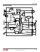
PIN FUNCTIONS
PGND (Pin 1): Power Ground. Ground return for the high
current gate drivers.
PG (Pin 2): Primary Gate. Gate drive for the primary
switch NMOS.
V
CC
(Pin 3): Main Supply Pin. A ceramic bypass capacitor
should be tied between this pin and ground.
AG (Pin 4): Active Gate. Gate drive for the active clamp
PMOS. This drive output is “in phase” with the PG out
-
put. Connect to the gate of a PMOS through a capacitive
level-shift cir
cuit.
I
SMAG
(Pin 5): Magnetizing Current Sense Pin. Connect
to a current sense resistor in series with the source of
the active clamp PMOS. This pin limits the magnetizing
current of the main transformer to prevent core saturation
when the active clamp is on.
DELAY (Pin 6): Primary Gate Rising Delay Adjustment. A
resistor from this pin to ground sets the AG rising to PG
rising dead time, which is critical for optimizing efficiency.
I
S
–
, I
S
+
(Pin 7, Pin 8): Inputs to the Overcurrent Compara-
tor. Connect across a current sense resistor in series with
the sour
ce of the primary NMOS.
FS/UV (Pin 10): Oscillator Frequency Set and Undervolt
-
age Indicator. A resistor to ground sets the switching
frequency during start-up. When the RUN pin is low,
the
V
CC
supply is undervoltage, or the overtemperature
protection is active, a 50µA current source pulls this pin
to the lesser of V
CC
and 5V as an indicator.
R
CORE
(Pin 11): Transformer Core Saturation Limit. A
resistor from R
CORE
to ground proportional to transformer
core parameters internally replicates the magnetizing cur-
rent slope
when the primary NMOS is on. This slope in
combination
with the voltage on the I
SMAG
and RUN pins
limits the on-time of the NMOS to prevent saturation. See
Applications Information.
RUN (Pin 12): Run Control and Undervoltage Lockout
(UVLO). Connect to a resistor divider to monitor the input
voltage V
IN
, which is required for proper operation of
the Direct Flux Limit. Converter operation is enabled for
V
RUN
>1.25V. Hysteresis is a fixed 50mV with an additional
5µA hysteresis current that combines with the resistor
divider to comprise the total UVLO hysteresis voltage.
SSFLT (Pin 13): Combination Soft-Start and Fault Indica
-
tor. A capacitor to ground sets the duty cycle ramp-up
rate
during primary-side start-up. To indicate a fault, the
SSFLT pin is momentarily pulled above 6V.
NDRV (Pin 14): Drive for External
Linear Regulator. Con-
nect to the gate of an NMOS and connect a pull-up resistor
to
the main input voltage, V
IN
. An internal charge pump
drives this pin above V
IN
for low input voltage applications.
IN
+
, IN
–
(Pin 15, Pin 16): Inputs from Pulse Transformer.
Connect through a DC restoring capacitor to the output
winding of a pulse transformer. The input winding of the
pulse transformer is driven by the LTC3766. After perform
-
ing an initial open-loop start-up, the LTC3765 detects and
decodes
pulse encoded PWM information at these pins,
and then turns control of the PG and AG switching over
to the LTC3766 secondary-side controller. Additionally,
an internal bridge rectifier on the IN
+
/IN
–
pins extracts
DC power from the pulse transformer and delivers it to
the V
CC
pin.
SGND (Pin 9, Exposed Pad Pin 17): Signal Ground. The
exposed pad metal of the package provides good thermal
contact to the printed circuit board. It must be soldered to
a ground plane for rated thermal performance.