
Datasheet

LTC3805
13
3805fg
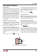
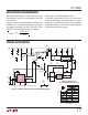
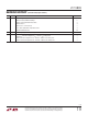
Figure 4. Setting RUN Pin Voltage and Run/Stop Control
LTC3805
RUN
RUN/STOP
CONTROL
(OPTIONAL)
R1
R2
GND
3805 F04
V
IN
applications inForMation
Leakage Inductance
Transformer leakage inductance (on either the primary
or secondary) causes a voltage spike to occur after the
MOSFET (Q1) turn-off. This is increasingly prominent at
higher load currents, where more stored energy must be
dissipated. In some cases an RC “snubber” circuit will be
required to avoid overvoltage breakdown at the MOSFET’s
drain node. Application Note 19 is a good reference on
snubber design. A bifilar or similar winding technique is a
good way to minimize troublesome leakage inductances.
However, remember that this will limit the primary-to-
secondary breakdown voltage, so bifilar winding is not
always practical.
Setting Undervoltage and Hysteresis on V
IN
The RUN pin is connected to a resistive voltage divider
connected to V
IN
as shown in Figure 4. The voltage thresh-
old for the RUN pin is V
RUNON
rising and V
RUNOFF
falling.
Note that V
RUNON
– V
RUNOFF
= 35mV of built-in voltage
hysteresis that helps eliminate false trips.
To introduce further user-programmable hysteresis, the
LTC3805 sources 5µA out of the RUN pin when operation
of LTC3805 is enabled. As a result, the falling threshold
for the RUN pin also depends on the value of R1 and can
be programmed by
the user. The falling threshold for V
IN
is therefore
V
IN(RUN,FALLING)
= V
RUNOFF
•
R1
+
R2
R2
− R1• 5µA
where R1(5µA) is the additional hysteresis introduced
by the 5µA current sourced by the RUN pin. When in
shutdown, the RUN pin does not source the 5µA current
and the rising threshold for V
IN
is simply
V
IN(RUN,RISING)
= V
RUNON
•
R1
+
R2
R2
External Run/Stop Control
To implement external run control, place a small N-channel
MOSFET from the RUN pin to GND as shown in Figure 4.
Drive the gate of this MOSFET high to pull the RUN pin
to ground and prevent converter operation.
Selecting Feedback Resistor Divider Values
The regulated output voltage is determined by the resistor
divider across V
OUT
(R3 and R4 in Figure 2). The ratio of R4
to R3 needed to produce a desired V
OUT
can be calculated:
R3 =
V
OUT
− 0.8V
0.8V
R4
Choose resistance values for R3 and R4 to be as large as
possible in order to minimize any efficiency loss due to
the static current drawn from V
OUT
, but just small enough
so that when V
OUT
is in regulation the input current to the
V
FB
pin is less than 1% of the current through R3 and R4.
A good rule of thumb is to choose R4 to be less than 80k.