
Datasheet

14
LTC3832/LTC3832-1
sn3832 3832fs
Note that the required R
DS(ON)
for Q2 is roughly three
times that of Q1 in this example. Note also that while the
required R
DS(ON)
values suggest large MOSFETs, the
power dissipation numbers are only 0.83W per device or
less; large TO-220 packages and heat sinks are not neces-
sarily required in high efficiency applications. Siliconix
Si4410DY or International Rectifier IRF7413 (both in
SO-8) or Siliconix SUD50N03-10 (TO-252) or ON Semi-
conductor MTD20N03HDL (DPAK) are small footprint
surface mount devices with R
DS(ON)
values below 0.03Ω
at 5V of V
GS
that work well in LTC3832 circuits. Using a
higher P
MAX
value in the R
DS(ON)
calculations generally
decreases the MOSFET cost and the circuit efficiency and
increases the MOSFET heat sink requirements.
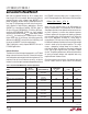
Table 1 highlights a variety of power MOSFETs for use in
LTC3832 applications.
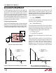
Inductor Selection
The inductor is often the largest component in an LTC3832
design and must be chosen carefully. Choose the inductor
value and type based on output slew rate requirements. The
maximum rate of rise of inductor current is set by the
inductor’s value, the input-to-output voltage differential and
the LTC3832’s maximum duty cycle. In a typical 3.3V in-
put, 2.5V output application, the maximum rise time will be:
DC V V
LL
A
s
MAX IN OUT
OO
•( – ) .
=
µ
076
where L
O
is the inductor value in µH. With proper fre-
quency compensation, the combination of the inductor
and output capacitor values determine the transient recov-
ery time. In general, a smaller value inductor improves
transient response at the expense of ripple and inductor
core saturation rating. A 1µH inductor has a 0.76A/µs rise
time in this application, resulting in a 6.6µs delay in
responding to a 5A load current step. During this 6.6µs,
the difference between the inductor current and the output
current is made up by the output capacitor. This action
causes a temporary voltage droop at the output. To
minimize this effect, the inductor value should usually be
in the 1µH to 5µH range for most 3.3V input LTC3832
circuits. To optimize performance, different combinations
of input and output voltages and expected loads may
require different inductor values.
Once the required value is known, the inductor core type
can be chosen based on peak current and efficiency
APPLICATIO S I FOR ATIO
WUUU
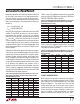
Table 1. Recommended MOSFETs for LTC3832 Applications
TYPICAL INPUT
R
DS(ON)
CAPACITANCE
PARTS AT 25°C (mΩ) RATED CURRENT (A) C
ISS
(pF) θ
JC
(°C/W) T
JMAX
(°C)
Siliconix SUD50N03-10 19 15 at 25°C 3200 1.8 175
TO-252 10 at 100°C
Siliconix Si4410DY 20 10 at 25°C 2700 150
SO-8 8 at 70°C
ON Semiconductor MTD20N03HDL 35 20 at 25°C 880 1.67 150
DPAK 16 at 100°C
Fairchild FDS6670A 8 13 at 25°C 3200 25 150
S0-8
Fairchild FDS6680 10 11.5 at 25°C 2070 25 150
SO-8
ON Semiconductor MTB75N03HDL 9 75 at 25°C 4025 1 150
DD PAK 59 at 100°C
IR IRL3103S 19 64 at 25°C 1600 1.4 175
DD PAK 45 at 100°C
IR IRLZ44 28 50 at 25°C 3300 1 175
TO-220 36 at 100°C
Fuji 2SK1388 37 35 at 25°C 1750 2.08 150
TO-220
Note: Please refer to the manufacturer’s data sheet for testing conditions and detailed information.