LTC3859A Low IQ, Triple Output, Buck/Buck/Boost Synchronous Controller with Improved Burst Mode Operation Description Features n n n n n n n n n n n n n n n Dual Buck Plus Single Boost Synchronous Controllers Outputs Remain in Regulation Through Cold Crank Down to 2.5V Low Operating IQ: 55μA (One Channel On) Wide Bias Input Voltage Range: 4.5V to 38V Buck Output Voltage Range: 0.
LTC3859A Absolute Maximum Ratings (Notes 1, 3) Bias Input Supply Voltage (VBIAS)............... –0.3V to 40V Buck Top Side Driver Voltages (BOOST1, BOOST2) .............................. –0.3V to 46V Boost Top Side Driver Voltages (BOOST3) ............................................. –0.3V to 76V Buck Switch Voltage (SW1, SW2) ................. –5V to 40V Boost Switch Voltage (SW3) ......................... –5V to 70V INTVCC, (BOOST1–SW1), (BOOST2–SW2), (BOOST3–SW3),........... –0.
LTC3859A Order Information LEAD FREE FINISH TAPE AND REEL PART MARKING* PACKAGE DESCRIPTION TEMPERATURE RANGE LTC3859AEFE#PBF LTC3859AEFE#TRPBF LTC3859AFE 38-Lead Plastic TSSOP –40°C to 125°C LTC3859AIFE#PBF LTC3859AIFE#TRPBF LTC3859AFE 38-Lead Plastic TSSOP –40°C to 125°C LTC3859AHFE#PBF LTC3859AHFE#TRPBF LTC3859AFE 38-Lead Plastic TSSOP –40°C to 150°C LTC3859AMPFE#PBF LTC3859AMPFE#TRPBF LTC3859AFE 38-Lead Plastic TSSOP –55°C to 150°C LTC3859AEUHF#PBF LTC3859AEUHF#TRPBF 3859A 38
LTC3859A Electrical Characteristics The l denotes the specifications which apply over the specified operating junction temperature range, otherwise specifications are at TA = 25°C. VBIAS = 12V, VRUN1,2,3 = 5V, EXTVCC = 0V unless otherwise noted. (Note 2) SYMBOL PARAMETER CONDITIONS IQ Input DC Supply Current (Note 5) Pulse-Skipping or Forced Continuous Mode (One Channel On) RUN1 = 5V and RUN2,3 = 0V or RUN2 = 5V and RUN1,3 = 0V or RUN3 = 5V and RUN1,2 = 0V VFB1, 2 ON = 0.83V (No Load) VFB3 = 1.
LTC3859A Electrical Characteristics The l denotes the specifications which apply over the specified operating junction temperature range, otherwise specifications are at TA = 25°C. VBIAS = 12V, VRUN1,2,3 = 5V, EXTVCC = 0V unless otherwise noted. (Note 2) SYMBOL PARAMETER CONDITIONS MIN TYP MAX UNITS Gate Driver TG1,2 Pull-Up On-Resistance Pull-Down On-Resistance 2.5 1.5 Ω Ω BG1,2 Pull-Up On-Resistance Pull-Down On-Resistance 2.4 1.1 Ω Ω TG3 Pull-Up On-Resistance Pull-Down On-Resistance 1.
LTC3859A Electrical Characteristics The l denotes the specifications which apply over the specified operating junction temperature range, otherwise specifications are at TA = 25°C. VBIAS = 12V, VRUN1,2,3 = 5V, EXTVCC = 0V unless otherwise noted. (Note 2) SYMBOL PARAMETER TPG1 Delay For Reporting a Fault CONDITIONS MIN TYP MAX 20 UNITS µs OV3 Boost Overvoltage Indicator Output VOV3L OV3 Voltage Low IOV3 = 2mA IOV3 OV3 Leakage Current VOV3 = 5V 0.
LTC3859A Typical Performance Characteristics Efficiency and Power Loss vs Output Current (Buck) Efficiency vs Output Current (Buck) 10000 90 90 60 100 50 FCM EFFICIENCY 10 PULSE-SKIPPING EFFICIENCY BURST LOSS 20 BURST EFFICIENCY 1 FCM LOSS 10 PULSE-SKIPPING LOSS 0.1 0 0.0001 0.001 0.1 0.
LTC3859A Typical Performance Characteristics Efficiency and Power Loss vs Output Current (Boost) Efficiency vs Output Current (Boost) 100 10000 90 90 100 50 FCM EFFICIENCY PULSE-SKIPPING 10 40 EFFICIENCY BURST LOSS 30 BURST 20 1 EFFICIENCY FCM LOSS 10 PULSE-SKIPPING LOSS 0.1 0 0.0001 0.001 0.1 0.
LTC3859A Typical Performance Characteristics 5.6 6.0 EXTVCC = 0V 5.4 INTVCC VOLTAGE (V) 5.4 INTVCC VOLTAGE (V) EXTVCC Switchover and INTVCC Voltages vs Temperature 5.3 5.2 5.1 5.8 EXTVCC AND INTVCC VOLTAGE (V) 5.5 INTVCC and EXTVCC vs Load Current INTVCC Line Regulation EXTVCC = 8.5V 5.2 5.0 4.8 EXTVCC = 5V 4.6 4.4 4.2 5.0 0 5 10 15 20 25 30 INPUT VOLTAGE (V) 35 4.0 40 20 60 80 40 LOAD CURRENT (mA) 3859A G19 5.0 4.6 4.
LTC3859A Typical Performance Characteristics Shutdown Current vs Input Voltage Shutdown Current vs Temperature VBIAS = 12V SHUTDOWN CURRENT (µA) 18 16 14 12 10 15 10 5 5 10 15 20 25 30 VBIAS INPUT VOLTAGE (V) 60 ONE CHANNEL ON 35 40 –75 –50 –25 40 0 25 50 75 100 125 150 TEMPERATURE (°C) 3859A G29 3859A G30 Undervoltage Lockout Threshold vs Temperature 600 4.4 4.3 FREQ = INTVCC 500 450 400 FREQ = GND 350 RISING 4.2 INTVCC VOLTAGE (V) 550 4.1 4.0 3.9 FALLING 3.8 3.7 3.6 3.
LTC3859A Pin Functions (QFN/TSSOP) FREQ (Pin 1/Pin 5): The Frequency Control Pin for the Internal VCO. Connecting the pin to GND forces the VCO to a fixed low frequency of 350kHz. Connecting the pin to INTVCC forces the VCO to a fixed high frequency of 535kHz. Other frequencies between 50kHz and 900kHz can be programmed using a resistor between FREQ and GND. The resistor and an internal 20µA source current create a voltage used by the internal oscillator to set the frequency.
LTC3859A pin functions (QFN/TSSOP) TRACK/SS1, TRACK/SS2, SS3 (Pins 34, 16, 3/Pins 38, 20, 7): External Tracking and Soft-Start Input. For the buck channels, the LTC3859A regulates the VFB1,2 voltage to the smaller of 0.8V, or the voltage on the TRACK/SS1,2 pin. For the boost channel, the LTC3859A regulates the VFB3 voltage to the smaller of 1.2V, or the voltage on the SS3 pin. An internal 1µA pull-up current source is connected to this pin.
4.7V EXTVCC VBIAS FREQ + – LDO LDO EN 5.4V SGND SYNC DET CLP VCO 5.4V EN 100k 20µA + – + – CLK1 CLK2 INTVCC PFD 0.72V VFB1 0.88V 6.8V RUN 11V SHDN RST 2(VFB) 6µA CH1 0.5µA CH2 + – BOT FOLDBACK SLEEP SHDN TOPON + – –+ SLOPE COMP 2.8V 0.65V Q R ICMP Q DROPOUT DET S BUCK CHANNELS 1 AND 2 3mV –+ PGOOD1 OV + – SHDN + – + EA – – IR SWITCHING LOGIC 1µA 0.88V PGND BG SW TG TRACK/SS ITH VFB SENSE– SENSE+ INTVCC 0.
OV3 + – VFB3 1.32V PLLIN/MODE CLK1 RUN3 Q R 11V 0.5µA SHDN + – SNSLO 1µA OV + – 2mV 1.32V + – SS3 ITH3 VFB3 SENSE3+ SENSE3– PGND BG3 SW3 TG3 3859A BD BOOST3 INTVCC 1.2V SS3 BOT TOP + EA – – 2V IR SWITCHING LOGIC + +– – SLEEP SHDN BOTON SNSLO + – –+ ICMP 0.425V Q S SLOPE COMP 2.8V 0.
LTC3859A Operation (Refer to Functional Diagram) Main Control Loop The LTC3859A uses a constant frequency, current mode step-down architecture. The two buck controllers, channels 1 and 2, operate 180 degrees out of phase with each other. The boost controller, channel 3, operates in phase with channel 1.
LTC3859A operation 0.8V internal reference for the bucks and the 1.2V internal reference for the boost, the LTC3859A regulates the VFB voltage to the TRACK/SS pin voltage instead of the corresponding reference voltage. This allows the TRACK/SS pin to be used to program a soft-start by connecting an external capacitor from the TRACK/SS pin to SGND. An internal 1µA pull-up current charges this capacitor creating a voltage ramp on the TRACK/SS pin. As the TRACK/SS voltage rises linearly from 0V to 0.8V/1.
LTC3859A Operation Frequency Selection and Phase-Locked Loop (FREQ and PLLIN/MODE Pins) The selection of switching frequency is a tradeoff between efficiency and component size. Low frequency operation increases efficiency by reducing MOSFET switching losses, but requires larger inductance and/or capacitance to maintain low output ripple voltage. The switching frequency of the LTC3859A’s controllers can be selected using the FREQ pin.
LTC3859A operation Buck Controller Output Overvoltage Protection Buck Foldback Current The two buck channels have an overvoltage comparator that guards against transient overshoots as well as other more serious conditions that may overvoltage their outputs. When the VFB1,2 pin rises by more than 10% above its regulation point of 0.800V, the top MOSFET is turned off and the bottom MOSFET is turned on until the overvoltage condition is cleared.
LTC3859A Operation 5V SWITCH 20V/DIV 3.3V SWITCH 20V/DIV INPUT CURRENT 5A/DIV INPUT VOLTAGE 500mV/DIV IIN(MEAS) = 2.53ARMS IIN(MEAS) = 1.55ARMS 3859A F01a (a) 3859A F01b (b) Figure 1. Input Waveforms Comparing Single-Phase (a) and 2-Phase (b) Operation for Dual Switching Regulators Converting 12V to 5V and 3.3V at 3A Each.
LTC3859A Applications Information The Typical Application on the first page is a basic LTC3859A application circuit. LTC3859A can be configured to use either DCR (inductor resistance) sensing or low value resistor sensing. The choice between the two current sensing schemes is largely a design trade-off between cost, power consumption, and accuracy. DCR sensing is becoming popular because it saves expensive current sensing resistors and is more power efficient, especially in high current applications.
LTC3859A Applications Information VIN1,2 (VOUT3) INTVCC BOOST TG LTC3859A SW RSENSE VOUT1,2 (VIN3) BG SENSE1,2+ (SENSE3–) SENSE1, 2– (SENSE3+) CAP PLACED NEAR SENSE PINS SGND 3859A F04a 4a. Using a Resistor to Sense Current VIN1,2 (VOUT3) INTVCC BOOST INDUCTOR TG LTC3859A SW L DCR VOUT1,2 (VIN3) BG SENSE1, 2+ (SENSE3–) SENSE1, 2– (SENSE3+) R1 C1* R2 SGND 3859A F04b *PLACE C1 NEAR SENSE PINS (R1||R2) • C1 = L/DCR RSENSE(EQ) = DCR(R2/(R1+R2)) 4b.
LTC3859A applications information The maximum power loss in R1 is related to duty cycle. For the buck controllers, the maximum power loss will occur in continuous mode at the maximum input voltage: (VIN(MAX) − VOUT ) • VOUT PLOSS R1= R1 Accepting larger values of DIL allows the use of low inductances, but results in higher output voltage ripple and greater core losses. A reasonable starting point for setting ripple current is DIL = 0.3(IMAX).
LTC3859A Applications Information Power MOSFET and Schottky Diode (Optional) Selection The MOSFET power dissipations at maximum output current are given by: Two external power MOSFETs must be selected for each controller in the LTC3859A: one N-channel MOSFET for the top switch (main switch for the buck, synchronous for the boost), and one N-channel MOSFET for the bottom switch (main switch for the boost, synchronous for the buck). The peak-to-peak drive levels are set by the INTVCC voltage.
LTC3859A applications information efficiency. The synchronous MOSFET losses for the buck controllers are greatest at high input voltage when the top switch duty factor is low or during a short-circuit when the synchronous switch is on close to 100% of the period. The synchronous MOSFET losses for the boost controller are greatest when the input voltage approaches the output voltage or during an overvoltage event when the synchronous switch is on 100% of the period.
LTC3859A Applications Information In continuous mode, the source current of the top MOSFET is a square wave of duty cycle (VOUT)/(VIN). To prevent large voltage transients, a low ESR capacitor sized for the maximum RMS current of one channel must be used. The maximum RMS capacitor current is given by: CIN Required IRMS ≈ IMAX ( VOUT ) ( VIN − VOUT )1/ 2 (1) VIN This formula has a maximum at VIN = 2VOUT, where IRMS = IOUT/2.
LTC3859A applications information Tracking and Soft-Start (TRACK/SS1, TRACK/SS2, SS3 Pins) tSS _ BUCK = CSS • 0.8V 1µA tSS _ BOOST = CSS • 1.2V 1µA Alternatively, the TRACK/SS1 and TRACK/SS2 pins for the two buck controllers can be used to track two (or more) supplies during start-up, as shown qualitatively in Figures 7a and 7b. To do this, a resistor divider should be connected from the master supply (VX) to the TRACK/SS pin of the slave supply (VOUT), as shown in Figure 8.
LTC3859A applications information INTVCC Regulators The LTC3859A features two separate internal P-channel low dropout linear regulators (LDO) that supply power at the INTVCC pin from either the VBIAS supply pin or the EXTVCC pin depending on the connection of the EXTVCC pin. INTVCC powers the gate drivers and much of the LTC3859A’s internal circuitry. The VBIAS LDO and the EXTVCC LDO regulate INTVCC to 5.4V. Each of these must be bypassed to ground with a minimum of 4.7µF ceramic capacitor.
LTC3859A Applications Information The following list summarizes the four possible connections for EXTVCC: 1. EXTVCC grounded. This will cause INTVCC to be powered from the internal 5.4V regulator resulting in an efficiency penalty of up to 10% at high input voltages. 2. EXTVCC connected directly to the output voltage of one of the buck regulators. This is the normal connection for a 5V to 14V regulator and provides the highest efficiency. 3. EXTVCC connected to an external supply.
LTC3859A applications information Topside MOSFET Driver Supply (CB, DB) External bootstrap capacitors CB connected to the BOOST pins supply the gate drive voltages for the topside MOSFETs. Capacitor CB in the Functional Diagram is charged though external diode DB from INTVCC when the SW pin is low. When one of the topside MOSFETs is to be turned on, the driver places the CB voltage across the gate-source of the desired MOSFET. This enhances the MOSFET and turns on the topside switch.
LTC3859A Applications Information Fault Conditions: Buck Current Limit and Current Foldback The LTC3859A includes current foldback for the buck channels to help limit load current when the output is shorted to ground. If the buck output falls below 70% of its nominal output level, then the maximum sense voltage is progressively lowered from 100% to 40% of its maximum selected value.
LTC3859A applications information If the external and internal frequencies are the same but exhibit a phase difference, the current sources turn on for an amount of time corresponding to the phase difference. The voltage at the VCO input is adjusted until the phase and frequency of the internal and external oscillators are identical. At the stable operating point, the phase detector output is high impedance and the internal filter capacitor, CLP, holds the voltage at the VCO input.
LTC3859A Applications Information Efficiency Considerations The percent efficiency of a switching regulator is equal to the output power divided by the input power times 100%. It is often useful to analyze individual losses to determine what is limiting the efficiency and which change would produce the most improvement. Percent efficiency can be expressed as: %Efficiency = 100% – (L1 + L2 + L3 + ...) where L1, L2, etc. are the individual losses as a percentage of input power.
LTC3859A applications information Checking Transient Response The regulator loop response can be checked by looking at the load current transient response. Switching regulators take several cycles to respond to a step in DC (resistive) load current. When a load step occurs, VOUT shifts by an amount equal to DILOAD(ESR), where ESR is the effective series resistance of COUT.
LTC3859A Applications Information Buck Design Example As a design example for one of the buck channels channel, assume VIN = 12V(NOMINAL), VIN = 22V(MAX), VOUT = 3.3V, IMAX = 6A, VSENSE(MAX) = 50mV, and f = 350kHz. The inductance value is chosen first based on a 30% ripple current assumption. The highest value of ripple current occurs at the maximum input voltage. Tie the FREQ pin to GND, generating 350kHz operation.
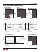
LTC3859A Applications Information PC Board Layout Checklist When laying out the printed circuit board, the following checklist should be used to ensure proper operation of the IC. These items are also illustrated graphically in the layout diagram of Figure 11. Figure 12 illustrates the current waveforms present in the various branches of the 2-phase synchronous buck regulators operating in the continuous mode. Check the following in your layout: 1.
LTC3859A Applications Information PC Board Layout Debugging Start with one controller on at a time. It is helpful to use a DC-50MHz current probe to monitor the current in the inductor while testing the circuit. Monitor the output switching node (SW pin) to synchronize the oscilloscope to the internal oscillator and probe the actual output voltage as well. Check for proper performance over the operating voltage and current range expected in the application.
LTC3859A Applications Information SW1 L1 D1 RSENSE1 VOUT1 COUT1 RL1 VIN RIN CIN SW2 BOLD LINES INDICATE HIGH SWITCHING CURRENT. KEEP LINES TO A MINIMUM LENGTH. D2 L2 RSENSE2 VOUT2 COUT2 RL2 3859A F11 Figure 11.
LTC3859A Typical Applications VOUT1 RB1 357k OPT RA1 68.1k VFB1 LTC3859A SENSE1– C1 1nF CITH1A 100pF SENSE1+ RITH1 15k CITH1 1500pF CSS1 0.1µF ITH1 PGOOD1 100k MTOP1 TG1 TRACK/SS1 FREQ PLLIN/MODE SW1 RUN1 RA2 68.1k RB2 649k 10pF RUN3 VOUT1 5V 5A COUT1 220µF D1 VBIAS CBIAS 10µF PGND VFB2 CITH2 2.2nF CINT1 4.7µF RITH2 15k ITH2 CITH2A 68pF C2 10µF INTVCC D2 TG2 CSS2 0.1µF TRACK/SS2 MTOP2 CB2 0.1µF BOOST2 L2 6.5µH RSENSE2 8mΩ SW2 VOUT3 RA3 68.
LTC3859A typical Applications VOUT1 RB1 475k 33pF RA1 34k VFB1 LTC3859A SENSE1– C1 1nF CITH1A 100pF SENSE1+ RITH1 10k CITH1 680pF ITH1 CSS1 0.1µF PGOOD1 FREQ PLLIN/MODE SW1 RUN1 RB2 215k 15pF RUN3 VOUT1 12V 3A COUT1 47µF D1 VBIAS CBIAS 10µF PGND VFB2 CITH2 820pF CINT1 4.7µF RITH2 15k ITH2 CITH2A 150pF C2 10µF INTVCC D2 TG2 CSS2 0.1µF TRACK/SS2 MTOP2 CB2 0.1µF BOOST2 L2 3.2µH RSENSE2 6mΩ SW2 VOUT3 RA3 68.1k RSENSE1 9mΩ MBOT1 BG1 RUN2 VOUT2 L1 8.8µH CB1 0.
LTC3859A typical Applications VOUT1 RA1 115k RB1 28.7k 56pF CITH1A 200pF LTC3859A SENSE1– C1 1nF SENSE1+ RITH1 3.93k CITH1 1000pF VFB1 ITH1 CSS1 0.01µF PGOOD1 FREQ PLLIN/MODE SW1 RUN1 RB2 57.6k 56pF RUN3 VOUT1 1V 8A COUT1 220µF ×2 D1 VBIAS CBIAS 10µF PGND VFB2 CITH2 1000pF CINT1 4.7µF RITH2 3.93k ITH2 CITH2A 200pF C2 10µF INTVCC D2 TG2 CSS2 0.01µF TRACK/SS2 MTOP2 CB2 0.1µF BOOST2 L2 0.47µH RSENSE2 3.5mΩ VOUT2 1.2V 8A SW2 VOUT3 RA3 12.1k RSENSE1 3.
LTC3859A typical Applications VOUT1 RB1 57.6k RA1 115k CITH1A 100pF LTC3859A SENSE1– C1 1nF SENSE1+ RITH1 5.6k CITH1 2.2nF VFB1 ITH1 CSS1 0.1µF PGOOD1 100k MTOP1 TG1 TRACK/SS1 FREQ PLLIN/MODE SW1 RUN1 RB2 357k RA2 115k RUN3 RSENSE1 9mΩ VOUT1 1.2V 3A COUT1 220µF MBOT1 BG1 D1 VBIAS CBIAS 10µF RUN2 VOUT2 L1 2.2µH CB1 0.1µF BOOST1 SGND C1 10µF PGND VFB2 CITH2 3.3nF CINT1 4.7µF RITH2 9.1k ITH2 CITH2A 100pF C2 10µF INTVCC D2 TG2 CSS2 0.1µF TRACK/SS2 MTOP2 CB2 0.
LTC3859A Package Description FE Package 38-Lead Plastic TSSOP (4.4mm) (Reference LTC DWG # 05-08-1772 Rev C) Exposed Pad Variation AA 4.75 REF 38 9.60 – 9.80* (.378 – .386) 4.75 REF (.187) 20 6.60 ±0.10 4.50 REF 2.74 REF SEE NOTE 4 6.40 2.74 REF (.252) (.108) BSC 0.315 ±0.05 1.05 ±0.10 0.50 BSC RECOMMENDED SOLDER PAD LAYOUT 4.30 – 4.50* (.169 – .177) 0.09 – 0.20 (.0035 – .0079) 0.50 – 0.75 (.020 – .030) NOTE: 1. CONTROLLING DIMENSION: MILLIMETERS 2. DIMENSIONS ARE IN MILLIMETERS (INCHES) 3.
LTC3859A Package Description UHF Package 38-Lead Plastic QFN (5mm × 7mm) (Reference LTC DWG # 05-08-1701 Rev C) 0.70 ± 0.05 5.50 ± 0.05 5.15 ± 0.05 4.10 ± 0.05 3.00 REF 3.15 ± 0.05 PACKAGE OUTLINE 0.25 ± 0.05 0.50 BSC 5.5 REF 6.10 ± 0.05 7.50 ± 0.05 RECOMMENDED SOLDER PAD LAYOUT APPLY SOLDER MASK TO AREAS THAT ARE NOT SOLDERED 5.00 ± 0.10 0.75 ± 0.05 PIN 1 NOTCH R = 0.30 TYP OR 0.35 × 45° CHAMFER 3.00 REF 37 0.00 – 0.05 38 0.40 ±0.10 PIN 1 TOP MARK (SEE NOTE 6) 1 2 5.15 ± 0.10 5.50 REF 7.
LTC3859A Typical Application High Efficiency Wide Input Range Dual 3.3V/8.5V Converter VOUT1 RB1 215k 15pF RA1 68.1k VFB1 LTC3859A SENSE1– C1 1nF CITH1A 150pF SENSE1+ RITH1 15k CITH1 820pF ITH1 CSS1 0.1µF PGOOD1 100k TRACK/SS1 FREQ PLLIN/MODE SW1 RUN1 RB2 649k 10pF RA2 68.1k RUN3 RSENSE1 6mΩ VOUT1 3.3V 5A COUT1 150µF MBOT1 BG1 D1 VBIAS CBIAS 10µF RUN2 VOUT2 L1 3.2µH CB1 0.1µF BOOST1 SGND C1 10µF MTOP1 TG1 PGND VFB2 CITH2 2.2nF CINT1 4.