
Datasheet


LTC3868
1
3868fd
TYPICAL APPLICATION
FEATURES
APPLICATIONS
DESCRIPTION
Low I
Q
, Dual
2-Phase Synchronous
Step-Down Controller
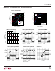
High Effi ciency Dual 8.5V/3.3V Step-Down Converter
n
Low Operating I
Q
: 170μA (One Channel On)
n
Wide Output Voltage Range: 0.8V ≤ V
OUT
≤ 14V
n
Wide V
IN
Range: 4V to 24V
n
R
SENSE
or DCR Current Sensing
n
Out-of-Phase Controllers Reduce Required Input
Capacitance and Power Supply Induced Noise
n
OPTI-LOOP
®
Compensation Minimizes C
OUT
n
Phase-Lockable Frequency (75kHz to 850kHz)
n
Programmable Fixed Frequency (50kHz to 900kHz)
n
Selectable Continuous, Pulse-Skipping or
Burst Mode
®
Operation at Light Loads
n
Very Low Dropout Operation: 99% Duty Cycle
n
Adjustable Output Voltage Soft-Start
n
Power Good Output Voltage Monitor
n
Output Overvoltage Protection
n
Output Latchoff Protection During Short Circuit
n
Low Shutdown I
Q
: 8µA
n
Internal LDO Powers Gate Drive from V
IN
or EXTV
CC
n
No Current Foldback During Start-Up
n
Small 5mm × 5mm QFN Package
n
Notebook and Palmtop Computers
n
Portable Instruments
n
Battery Operated Digital Devices
n
Distributed DC Power Systems
L, LT, LTC, LTM, Burst Mode, OPTI-LOOP, PolyPhase, µModule, Linear Technology and the Linear
logo are registered trademarks and No R
SENSE
and UltraFast are trademarks of Linear Technology
Corporation. All other trademarks are the property of their respective owners. Protected by U.S.
Patents, including 5481178, 5705919, 5929620, 6100678, 6144194, 6177787, 6304066, 6580258.
Effi ciency and Power Loss
vs Load Current
The LTC
®
3868 is a high performance dual step-down
switching regulator controller that drives all N-channel
synchronous power MOSFET stages. A constant frequency
current mode architecture allows a phase-lockable fre-
quency of up to 850kHz. Power loss and noise due to the
input capacitor ESR are minimized by operating the two
controller outputs out of phase.
The 170A no-load quiescent current extends operating life in
battery-powered systems. OPTI-LOOP compensation allows
the transient response to be optimized over a wide range of
output capacitance and ESR values. The LTC3868 features a
precision 0.8V reference and a power good output indicator. A
wide 4V to 24V input supply range encompasses a wide range
of intermediate bus voltages and battery chemistries.
Independent soft-start pins for each controller ramp the
output voltages during start-up. Current foldback limits
MOSFET heat dissipation during short-circuit conditions.
The output short-circuit latchoff feature further protects
the circuit in short-circuit conditions.
For a leaded 28-lead SSOP package with a fi xed current
limit and one PGOOD output, without phase modulation
or a clock output, see the LTC3868-1 data sheet.
0.1µF
62.5k
3.3µH
680pF
150µF
4.7µF
22µF
50V
0.007Ω
20k
15k
V
OUT1
3.3V
5A
150µF
0.1µF
193k
7.2µH
680pF
0.01Ω
20k
15k
V
OUT2
8.5V
3.5A
TG1 TG2
BOOST1 BOOST2
SW1 SW2
BG1 BG2
SGND
PGND
SENSE1
+
SENSE2
+
SENSE1
–
SENSE2
–
V
FB1
V
FB2
I
TH1
I
TH2
V
IN
INTV
CC
SS1 SS2
V
IN
9V TO 24V
3868 TA01
0.1µF
0.1µF
LTC3868
OUTPUT CURRENT (A)
0.0001
40
EFFICIENCY (%)
POWER LOSS (mW)
50
60
70
80
0.001 0.01 0.1 1 10
3868 TA01b
30
20
10
0
90
100
10
100
1000
1
0.1
10000
EFFICIENCY
POWER LOSS
V
IN
= 12V
V
OUT
= 3.3V
FIGURE 12 CIRCUIT