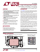
LTC4000 High Voltage High Current Controller for Battery Charging and Power Management Description Features n n n n n n n n n n Complete High Performance Battery Charger When Paired with a DC/DC Converter Wide Input and Output Voltage Range: 3V to 60V Input Ideal Diode for Low Loss Reverse Blocking and Load Sharing Output Ideal Diode for Low Loss PowerPath™ and Load Sharing with the Battery Instant-On Operation with Heavily Discharged Battery Programmable Input and Charge Current: ±1% Accuracy ±0.
LTC4000 Absolute Maximum Ratings (Note 1) IN, CLN, IID, CSP, CSN, BAT........................ –0.3V to 62V IN-CLN, CSP-CSN.............................................–1V to 1V OFB, BFB, FBG............................................ –0.3V to 62V FBG.............................................................–1mA to 2mA IGATE............Max (VIID, VCSP) – 10V to Max (VIID, VCSP) BGATE........Max (VBAT, VCSN) – 10V to Max (VBAT, VCSN) ENC, CX, NTC, VM....................................–0.
LTC4000 Electrical Characteristics The l denotes the specifications which apply over the full operating junction temperature range, otherwise specifications are at TA = 25°C. VIN = VCLN = 3V to 60V unless otherwise noted (Notes 2, 3). SYMBOL PARAMETER VIN Input Supply Operating Range IIN Input Quiescent Operating Current IBAT Battery Pin Operating Current Battery Only Quiescent Current CONDITIONS MIN l TYP 3 MAX 60 0.
LTC4000 Electrical Characteristics The l denotes the specifications which apply over the full operating junction temperature range, otherwise specifications are at TA = 25°C. VIN = VCLN = 3V to 60V unless otherwise noted (Notes 2, 3). SYMBOL PARAMETER CONDITIONS MIN TYP MAX UNITS Charge Termination CX Pin Pull-Up Current VCX = 0.1V l –5.5 –5.0 –4.5 µA VCX,IBMON(OS) CX Comparator Offset Voltage, IBMON Falling VCX = 0.1V l 0.
LTC4000 Electrical Characteristics The l denotes the specifications which apply over the full operating junction temperature range, otherwise specifications are at TA = 25°C. VIN = VCLN = 3V to 60V unless otherwise noted (Notes 2, 3). SYMBOL PARAMETER CONDITIONS MIN TYP MAX UNITS Battery PowerPath Control Battery Discharge PowerPath Forward Regulation Voltage VBAT,CSN, 2.8V ≤ VBAT ≤ 60V l 0.1 8 20 mV Battery PowerPath Fast Reverse Turn-Off Threshold Voltage VBAT,CSN, 2.
LTC4000 Typical Performance Characteristics Input Quiescent Current and Battery Quiescent Current Over Temperature 1.0 Battery Float Voltage Feedback, Output Voltage Regulation Feedback and VM Falling Threshold Over Temperature Battery Only Quiescent Current Over Temperature 100 VIN = VBAT = 15V VCSN = 15.5V IIN 1.20 1.19 VBAT = 60V 10 1.18 IBAT PIN VOLTAGE (V) 0.1 1 IBAT (µA) IIN/IBAT (mA) VBAT = 15V VBAT = 3V 0.1 0.01 1.17 VVM(TH) VOFB_REG 1.16 1.15 1.14 VBFB_REG 1.13 1.12 1.
LTC4000 Typical Performance Characteristics Charge Termination Time with 0.1µF Timer Capacitor Over Temperature 3.5 80 VNTC(COLD) 75 3.3 14 12 2.9 2.7 VIID,CSP / VBAT,CSN (mV) PERCENT OF VBIAS (%) 70 3.1 TT (h) PowerPath Forward Voltage Regulation Over Temperature NTC Thresholds Over Temperature 65 60 55 VNTC(OPEN) 50 45 VNTC(HOT) 40 2.5 VIGATE (ON)/VBGATE(ON) (V) 0 –30 14.0 13.5 13.0 12.5 12.0 –60 11.5 –90 –60 –40 –20 0 20 40 60 80 100 120 140 TEMPERATURE (°C) 11.
LTC4000 Pin Functions (QFN/SSOP) VM (Pin 1/Pin 25): Voltage Monitor Input. High impedance input to an accurate comparator with a 1.193V threshold (typical). This pin controls the state of the RST output pin. Connect a resistor divider (RVM1, RVM2) between the monitored voltage and GND, with the center tap point connected to this pin. The falling threshold of the monitored voltage is calculated as follows: VVM _ RST = RVM1 + RVM2 • 1.
LTC4000 Pin Functions (QFN/SSOP) is not exceeded. The charge current limit is determined using the following formula: R ICLIM = 2.5µA • CL RCS Where RCS is the sense resistor connected to the CSP and the CSN pins. Leave the pin open for the maximum charge current limit of 50mV/RCS. TMR (Pin 9/Pin 5): Charge Timer. Attach 1nF of external capacitance (CTMR) to GND for each 104 seconds of charge termination time and 26 seconds of bad battery indicator time.
LTC4000 Pin Functions (QFN/SSOP) CSN (Pin 19/Pin 15): Charge Current Sense Negative Input and Battery Ideal Diode Cathode. Connect a sense resistor between this pin and the CSP pin. The LTC4000 senses the voltage across this sense resistor and regulates it to a voltage equal to 1/20th (typical) of the voltage set at the CL pin. The maximum regulated sense voltage is 50mV. The CSN pin is also the cathode input of the battery ideal diode driver (the anode input is the BAT pin).
LTC4000 Block Diagram RIS CIN CIID RC IN CLN RST VM – CIBMON CC ITH CC IID IBMON IGATE CSP CP1 RVM2 1.193V 8mV + + – – + A8 gm = 0.33m A9 gm = 0.33m 60k A1 +– INPUT IDEAL DIODE DRIVER 8mV gm A11 60k 50µA RIL A4 IL 1V + –gm – gm– BIAS A5 – CL – A7 + – A6 + – REF gm BIAS RCL OFB gm OFB 1.193V CP6 BFB – 0.771V ROFB2 1.136V + BFB CP5 NTC + TOO COLD – RBFB2 1.
LTC4000 Operation Overview The LTC4000 is designed to simplify the conversion of any externally compensated DC/DC converter into a high performance battery charger with PowerPath control. It only requires the DC/DC converter to have a control or external-compensation pin (usually named VC or ITH) whose voltage level varies in a positive monotonic way with its output. The output variable can be either output voltage or output current. For the following discussion, refer to the Block Diagram in Figure 1.
LTC4000 Operation CSP pin (source). The controller (A1) regulates the external PMOS by driving the gate of the PMOS device such that the voltage drop across IID and CSP is 8mV (typical). When the external PMOS ability to deliver a particular current with an 8mV drop across its source and drain is exceeded, the voltage at the gate clamps at VIGATE(ON) and the PMOS behaves like a fixed value resistor (RDS(ON)).
LTC4000 Operation If the system load requires more power than is available from the input, the battery ideal diode controller provides supplemental power from the battery. When the battery voltage discharges below 97.1% of the float voltage (VBFB < VRECHRG(FALL)), the automatic recharge feature initiates a new charge cycle. RBFB1 RBFB2 BAT LTC4000 BFB + – FBG 1.136V A6 CC CC – + RC ITH TO DC/DC 4000 FO4 Charge Current Regulation Figure 4.
LTC4000 Operation behavior, BGATE also allows current to flow from the CSN pin to the BAT pin during charging. There are two regions of operation when current is flowing from the CSN pin to the BAT pin. The first is when charging into a battery whose voltage is below the instant-on threshold (VOFB < VOUT(INST_ON)). In this region of operation, the controller regulates the voltage at the CSP pin to be approximately 86% of the final float voltage level (VOUT(INST_ON)).
LTC4000 Applications Information Input Ideal Diode PMOS Selection The input external PMOS is selected based on the expected maximum current, power dissipation and reverse voltage drop. The PMOS must be able to withstand a gate to source voltage greater than VIGATE(ON) (15V maximum) or the maximum regulated voltage at the IID pin, whichever is less. A few appropriate external PMOS for a number of different requirements are shown at Table 1. Table 1. PMOS RDS(ON) AT VGS = 10V (Ω) MAX ID (A) SiA923EDJ 0.
LTC4000 Applications Information The voltage on the IIMON pin can be filtered further by putting a capacitor on the pin (CIIMON). The voltage on the IIMON pin is also the feedback input to the input current regulation error amplifier. Any capacitor connected to this pin places a pole in the input current regulation loop. Therefore, this filter capacitor should NOT be arbitrarily large as it will slow down the overall compensated loop.
LTC4000 Applications Information Once the battery voltage rises above the low battery voltage threshold, the charge current level rises from the trickle charge current level to the full charge current level. The LTC4000 also features bad battery detection. This detection is disabled if the TMR pin is grounded or tied to BIAS. However, when a capacitor is connected to the TMR pin, a bad battery detection timer is started as soon as trickle charging starts.
LTC4000 Applications Information Battery Instant-On and Ideal Diode External PMOS Consideration On the other hand, when the battery voltage is above the low battery threshold but still below the instant-on threshold, the power dissipation can be calculated as follows: The instant-on voltage level is determined using the following formula: PINST _ ON = [0.86 • VFLOAT – VBAT ] • ICLIM ROFB1 + ROFB2 • 0.
LTC4000 Applications Information Similar to the input external PMOS, the charging external PMOS must be able to withstand a gate to source voltage greater than VBGATE(ON) (15V maximum) or the maximum regulated voltage at the CSP pin, whichever is less. Consider the expected maximum current, power dissipation and instant-on voltage drop when selecting this PMOS. The PMOS suggestions in Table 1 are an appropriate starting point depending on the application.
LTC4000 Applications Information Battery Temperature Qualified Charging To use the battery temperature qualified charging feature, connect an NTC thermistor, RNTC, between the NTC pin and the GND pin, and a bias resistor, R3, from the BIAS pin to the NTC pin (Figure 9). Thermistor manufacturer datasheets usually include either a temperature lookup table or a formula relating temperature to the resistor value at that corresponding temperature.
LTC4000 Applications Information The value of R3 and RD can now be set according to the following formula: R at cold_ threshold – RNTC at hot _ threshold R3 = NTC 2.461 RD = 0.219 • RNTC at cold_ threshold – 1.219 • RNTC at hot _ threshold Note the important caveat that this method can only be used to desensitize the thermal effect on the thermistor and hence push the hot and cold temperature thresholds apart from each other.
LTC4000 Applications Information Setting the Input Voltage Monitoring Resistor Divider The falling threshold voltage level for this monitoring function can be calculated as follows: V RVM1 = VM _ RST – 1 • R VM2 1.193V where RVM1 and RVM2 form a resistor divider connected between the monitored voltage and GND, with the center tap point connected to the VM pin as shown in Figure 6. The rising threshold voltage level can be calculated similarly.
LTC4000 Applications Information SWITCHING CONVERTER GND ITH 1k 0.015µF RC CC CLN ITH CC IOUT CSP LTC4000 IN A 10k B 1500pF 50Ω 1W 1000µF (OBSERVE POLARITY) SCOPE GROUND CLIP CSN GND BAT BGATE 50Ω GENERATOR f = 50Hz VIN 4000 F12 Figure 12. Empirical Loop Compensation Setup Generator frequency is set at 50Hz. Lower frequencies may cause a blinking scope display and higher frequencies may not allow sufficient settling time for the output transient.
LTC4000 Applications Information GENERATOR OUTPUT REGULATOR OUTPUT WITH LARGE CC, SMALL RC WITH REDUCED CC, SMALL RC EFFECT OF INCREASED RC FURTHER REDUCTION IN CC MAY BE POSSIBLE IMPROPER VALUES WILL CAUSE OSCILLATIONS 4000 F13 Figure 13. Typical Output Transient Response at Various Stability Level If the regulator response is under damped with the initial large value of CC, RC should be increased immediately before larger values of CC are tried.
LTC4000 Applications Information Design Example In this design example, the LTC4000 is paired with the LT3845A buck converter to create a 10A, 3-cell LiFePO4 battery charger. The circuit is shown on the front page and is repeated here in Figure 14. • RCL is set at 24.9kΩ such that the voltage at the CL pin is 1.25V. Similar to the IIMON pin, the regulation voltage on the IBMON pin is clamped at 1V with an accurate internal reference.
LTC4000 Applications Information • The charge termination time is set at 2.9 hours according to the following formula: CTMR (nF) = t TERMINATE (h) • 34.6 = 2.9 • 34.6 = 100nF • The C/X current termination level is programmed at 1A according to the following formula: RCX = (1A • 5mΩ) + 0.5mV ≈ 22.1kΩ 0.25µA Note that in this particular solution, the timer termination is selected since a capacitor connects to the TMR pin. Therefore, this C/X current termination level only applies to the CHRG indicator pin.
LTC4000 Applications Information With CC = 1µF, RC = 10k at VIN = 20V, VBAT = 7V, VCSP regulated at 9.8V and a 0.2A output load condition at CSP, the transient response for a 100mA charge current step observed at IBMON is shown in Figure 16. 10 15 5 10 0 5 VIBMON (mV) 5mV/DIV VIBMON (mV) 5mV/DIV 15 The transient response now indicates an overall under damped system. As noted in the empirical loop compensation section, the value of RC is now increased iteratively until RC = 20k.
LTC4000 Applications Information This same procedure is then repeated for the other four loops: the input current regulation, the output voltage regulation, the battery float voltage regulation and finally the charge current regulation when VOFB > VOUT(INST_ON). Note that the resulting optimum values for each of the loops may differ slightly. The final values of CC and RC are then selected by combining the results and ensuring the most conservative response for all the loops.
LTC4000 Applications Information Appendix—The Loop Transfer Functions The Input Current Regulation Loop When a series resistor (RC) and capacitor (CC) is used as the compensation network as shown in Figure 11, the transfer function from the input of A4-A7 to the ITH pin is simply as follows: The feedback signal for the input current regulation loop is the sense voltage across the input current sense resistor (RIS). where gm4-7 is the transconductance of error amplifier A4A7, typically 0.
LTC4000 Applications Information The Output Voltage Regulation Loop The Battery Float Voltage Regulation Loop The feedback signal for the output voltage regulation loop is the voltage on the OFB pin, which is connected to the center node of the resistor divider between the output voltage (connected to CSP) and the FBG pin. This voltage is compared to an internal reference (1.193V typical) by the transconductance error amplifier A7.
LTC4000 Applications Information In Figure 22 the battery is approximated to be a signal ground in series with the internal battery resistance RBAT.
LTC4000 Applications Information The Battery Charge Current Regulation Loop when VOFB is Regulated to VOUT(INST_ON) The simplified loop transmission is: When the battery voltage is below the instant-on level, the external charging PFET is driven linearly to regulate the voltage at the output (connected to the CSP pin). The output voltage is regulated such that the voltage at the OFB pin is equal to the instant-on threshold (VOUT(INST_ON)).
LTC4000 Typical Applications VIN 15V TO 60V 10A MAX 5mΩ 2.2µF BSC123NO8NS3 47µF VIN TG WÜRTH ELEKTRONIC 74435561100 10µH SW BG CSS B160 Si7135DP 3mΩ BSC123NO8NS3 0.1µF 1.5nF SYNC 33µF ×3 VOUT 12V, 15A 10M BOOST BAS521 SGND 1.15M VCC 1µF LT3845A 49.9k 1N4148 182k VFB fSET 16.2k BURST_EN SENSE+ SHDN VC SENSE BIAS 1M 5mΩ – 14.7k RST ITH NTHS0603 N02N1002J 47nF CC IID IGATE CSP CSN BGATE CLN IN 1.
LTC4000 Typical Applications VIN 6V TO 18V 15A MAX 3.3mΩ 2.5mΩ 150µF 22µF ×4 PA1494.362NL 3.3µH 10Ω 1nF 10Ω INTVCC Si7135DP BSC027N04 SENSE+ 22µF ×5 BOOST INTVCC PLLINMODE 100k INTVCC LTC3786 RUN SS 0.1µF FREQ 0.1µF 1.87M BSC027N04 TG VBIAS 232k VFB GND 10M 150µF SW BG PGOOD 4.7µF VOUT 22V, 5A BAS140W SENSE– ITH 12.1k 10mΩ 28.
VIN 18V TO 72V 2.2µF ×2 36 0.1µF 15.8k 221k FS VCC 681Ω For more information www.linear.com/LTC4000 13.6k 0.04Ω VCC 150pF ISO1 PS2801-1-K BAS516 3.01k 68Ω BAS516 • • • BAS516 1.5k VOUT PDS1040 VOUT 10nF 24.9k 47nF VM 150k IN 10nF IIMON IBMON IL CL ENC CHRG FLT RST ITH CC 100k 100µF ×3 22.1k TMR 100nF LTC4000 CLN 1µF 20mΩ CX NTC FBG BFB OFB BAT BGATE CSN CSP IGATE GND BIAS 22.1k IID SiA923EDJ Figure 27. 18V to 72VIN to 4.2V at 2.
LTC4000 Package Description Please refer to http://www.linear.com/designtools/packaging/ for the most recent package drawings. UFD Package 28-Lead Plastic QFN (4mm × 5mm) (Reference LTC DWG # 05-08-1712 Rev B) 0.70 ±0.05 4.50 ±0.05 3.10 ±0.05 2.50 REF 2.65 ±0.05 3.65 ±0.05 PACKAGE OUTLINE 0.25 ±0.05 0.50 BSC 3.50 REF 4.10 ±0.05 5.50 ±0.05 RECOMMENDED SOLDER PAD PITCH AND DIMENSIONS APPLY SOLDER MASK TO AREAS THAT ARE NOT SOLDERED 4.00 ±0.10 (2 SIDES) 0.75 ±0.05 R = 0.05 TYP PIN 1 NOTCH R = 0.
LTC4000 Package Description Please refer to http://www.linear.com/designtools/packaging/ for the most recent package drawings. GN Package 28-Lead Plastic SSOP (Narrow .150 Inch) (Reference LTC DWG # 05-08-1641 Rev B) .386 – .393* (9.804 – 9.982) .045 ±.005 28 27 26 25 24 23 22 21 20 19 18 17 1615 .254 MIN .033 (0.838) REF .150 – .165 .229 – .244 (5.817 – 6.198) .0165 ±.0015 .150 – .157** (3.810 – 3.988) .0250 BSC 1 RECOMMENDED SOLDER PAD LAYOUT .015 ±.004 × 45° (0.38 ±0.10) .0075 – .0098 (0.
LTC4000 Revision History REV DATE DESCRIPTION PAGE NUMBER A 5/11 Updated the Typical Application. Updated the Electrical Characteristics section. B 6/13 1 3, 4, 5 Updated the ENC pin text in the Pin Functions section. 8 Updated the Block Diagram. 11 Updated Figures 14 and 25. 26, 34 Added Common Mode Range spec to CLN, CSP and CSN. 3 Revised Ratio of Monitored-Current Voltage to Sense Voltage min 3 Revised VBFB_REG Battery Feedback Voltage min.
LTC4000 Typical Application 5.6Ω IHLP6767GZ ER4R7M01 4.7µH 390pF 3.6Ω B240A VIN 6V TO 36V 12.5A MAX 4mΩ Q2 270µF Q4 B240A Q5 0.22µF TG1 SW1 0.01Ω Q3 Si7135DP 330µF ×2 0.22µF 0.01Ω 1.24k 3.3µF ×5 1800pF 1.24k BG1 SENSE+ SENSE– BG2 SW2 BOOST1 VOUT 15V, 5A 10M 22µF ×2 TG2 BOOST2 DFLS160 DFLS160 INTVCC INTVCC 10µF MODE/PLLIN VIN 1µF 100k LTC3789 VINSNS PGOOD 309k IOSENSE+ IOSENSE– VOUTSNS BZT52C5V6 121k FREQ EXTVCC ILIM RUN ITH SS SGND 8.06k 10mΩ 10nF 14.