
Datasheet


13
LTC4011
4011fa
OPERATIO
U
12
–
+
CC
EA
I
TH
I
PROG
R3
Q
PWM CLOCK
S
R
R4
R1
BAT
11
SENSE
R
SENSE
15
BGATE
17
TGATE
LTC4011
V
CC
P
N
R2
4011 F02
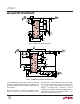
Figure 2. LTC4011 PWM Control Loop
PWM Current Source Controller
An integral part of the LTC4011 is the PWM current source
controller. The charger uses a synchronous step-down
architecture to produce high efficiency and limited thermal
dissipation. The nominal operating frequency of 550kHz
allows use of a smaller external filter components. The
TGATE and BGATE outputs have internally clamped volt-
age swings. They source peak currents tailored to smaller
surface-mount power FETs likely to appear in applications
providing an average charge current of 3A or less. During
the various charging states, the LTC4011 uses the PWM
controller to regulate an average voltage between SENSE
and BAT that ranges from 10mV to 100mV.
A conceptual diagram of the LTC4011 PWM control loop
is shown in Figure 2.
The voltage across the external current programming
resistor R
SENSE
is averaged by integrating error amplifier
EA. An internal programming current is also pulled from
input resistor R1. The I
PROG
• R1 product establishes the
desired average voltage drop across R
SENSE
, and hence,
the average current through R
SENSE
. The I
TH
output of the
error amplifier is a scaled control current for the input of
the PWM comparator CC. The I
TH
• R3 product sets a peak
current threshold for CC such that the desired average
current through R
SENSE
is maintained. The current com-
parator output does this by switching the state of the SR
latch at the appropriate time.
At
the beginning of each oscillator cycle, the PWM clock
sets the SR latch and the external P
-channel
MOSFET is
switched on (N
-channel
MOSFET switched off) to refresh
the current carried by the external inductor. The inductor
current and voltage drop across R
SENSE
begin to rise
linearly. During normal operation, the PFET is turned off
(NFET on) during the cycle by CC when the voltage
difference across R
SENSE
reaches the peak value set by
the output of EA. The inductor current then ramps down
linearly until the next rising PWM clock edge. This closes
the loop and maintains the desired average charge current
in the external inductor.
Low Dropout Charging
After charging is initiated, the LTC4011 does not require
that V
CC
remain at least 500mV above BAT because
situations exist where low dropout charging might occur.
In one instance, parasitic series resistance may limit PWM
headroom (between V
CC
and BAT) as 100% charge is
reached. A second case can arise when the DC adapter
selected by the end user is not capable of delivering the
current programmed by R
SENSE
, causing the output volt-
age of the adapter to collapse. While in low dropout, the
LTC4011 PWM runs near 100% duty cycle with a fre-
quency that may not be constant and can be less than
550kHz. The charge current will drop below the pro-
grammed value to avoid generating audible noise, so the
actual charge delivered to the battery may depend prima-
rily on the LTC4011 charge timer.
Internal Die Temperature
The LTC4011 provides internal overtemperature detec-
tion to protect against electrical overstress, primarily at
the FET driver outputs. If the die temperature rises above
this thermal limit, the LTC4011 stops switching and
indicates a fault as previously discussed.