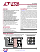
LTC4020 55V Buck-Boost Multi-Chemistry Battery Charger Features Description Wide Voltage Range: 4.5V to 55V Input, Up to 55V Output (60V Absolute Maximums) nn Synchronous Buck-Boost DC/DC Controller nn Li-Ion and Lead-Acid Charge Algorithms nn ±0.
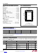
LTC4020 Absolute Maximum Ratings Pin Configuration (Note 1) SW2 BG2 INTVCC PGND PVIN SW1 BG1 TOP VIEW PVIN, SENSVIN.............................................. –0.3 to 60V BST1, BST2................................................... –0.3 to 66V SW1, SW2.........................................................–2 to 60V SENSVIN – PVIN............................................ –0.3 to 60V BST1 – SW1, BST2 – SW2.............................. –0.3 to 6V SENSVIN – SENSTOP, SENSBOT – SENSGND.......
LTC4020 Electrical Characteristics The l denotes the specifications which apply over the specified operating junction temperature range, otherwise specifications are at TA = 25°C (Note 2). PVIN = SENSVIN = CSP = CSN = BAT = 20V, SHDN = 2V, C(TG1, BG1, TG2, BG2) = 1000pF, VRNG/SS = 2V. SYMBOL INTVCC IPVIN ISENSVIN PARAMETER CONDITIONS 5.15 V Boost Refresh Supply Short-Circuit Current Limit VINTVCC = 0V l PVIN Operating Current Note 3; ITH = 0V l Shutdown Current VSHDN = 0 l 3 6 µA l 0.
LTC4020 Electrical Characteristics The l denotes the specifications which apply over the specified operating junction temperature range, otherwise specifications are at TA = 25°C (Note 2). PVIN = SENSVIN = CSP = CSN = BAT = 20V, SHDN = 2V, C(TG1, BG1, TG2, BG2) = 1000pF, VRNG/SS = 2V.
LTC4020 Electrical Characteristics The l denotes the specifications which apply over the specified operating junction temperature range, otherwise specifications are at TA = 25°C (Note 2). PVIN = SENSVIN = CSP = CSN = BAT = 20V, SHDN = 2V, C(TG1, BG1, TG2, BG2) = 1000pF, VRNG/SS = 2V.
LTC4020 Typical Performance Characteristics VFLOAT(CC/CV) or, VABSORB(Lead-Acid) Reference vs Temperature VFLOAT(Lead-Acid) Reference vs Temperature VFBMAX Reference vs Temperature 2.525 2.36 2.80 2.520 2.35 2.79 2.515 2.34 2.78 2.33 2.505 2.500 2.495 2.77 2.32 VOLTAGE (V) VOLTAGE (V) 2.510 VOLTAGE (V) TA = 25°C, unless otherwise noted. 2.31 2.30 2.29 2.76 2.75 2.74 2.490 2.28 2.73 2.485 2.27 2.72 2.480 2.26 2.71 2.
LTC4020 Typical Performance Characteristics Ideal Diode VF vs Temperature Ideal Diode VF vs Battery Voltage 16.0 24 15.5 14.5 14.0 13.5 13.0 4.4 25°C 18 16 0 125°C Feedback References vs Input Voltage CSOUT vs CSP-CSN 2.80 1.2 2.75 1.1 2.70 FEEDBACK REFERENCES (V) 1.3 0.9 0.8 0.7 0.6 0.5 0.4 0.3 20 30 V(CSP-CSN) (mV) 40 2.55 255 2.45 5.02 5.00 4.98 4.96 2.40 2.35 4.94 VFLOAT(LEAD-ACID) 4.92 5 4.
LTC4020 Pin Functions TG1 (Pin 1): VIN side (step-down) primary switch FET gate driver output. BST1 (Pin 2): Boosted supply rail for VIN side (step-down) switch FETs. Connect 1µF capacitor from this pin to SW1. Connect 1A Schottky diode cathode to this pin, anode to INTVCC pin. SENSGND (Pin 4): Kelvin connection for PGND used for SENSBOT current sense reference. SENSBOT (Pin 5): Ground Referred Current Sense Amplifier Input.
LTC4020 Pin Functions is terminated or when charge current is below the C/10 threshold. If the LTC4020 is configured for a CC charging algorithm, the STAT1 pin is pulled low during the entire charging cycle. The STAT1 pin becomes high impedance when the charge cycle is terminated. If the LTC4020 is configured for a lead-acid charging algorithm, the STAT1 pin is used as a charge cycle stage indicator pin, and pulled low during the bulk and absorption charging stages.
LTC4020 Pin Functions The RNG/SS pin is pulled low during periods when charging is disabled, including NTC faults, bad battery faults, and normal charge cycle termination. This allows for a graceful start after faults and when initiating new charge cycles, should soft-start functionality be implemented. Both a soft-start capacitor and a programming resistor can be implemented in parallel.
LTC4020 Pin Functions Using the same resistor values for battery voltage programming, or RFB1 = RMIN1 and RFB2 = RMIN2, yields an instant-on voltage that is 85% of VFLOAT (CC/CV charging) or VABSORB (lead-acid charging): VOUT(MIN) = 0.85 • VFLOAT/ABSORB BAT (Pin 20): Battery Voltage Monitor Pin. This pin serves as the positive reference for the LTC4020 ideal diode function.
LTC4020 Pin Functions Pin output impedance is 100kΩ, so any loading for monitors must be high impedance. The sense output voltage follows the relation: VCSOUT = 0.25 + 20 • (VCSP – VCSN) CSOUT is only active while battery charger functions are operating. CSOUT pin voltage is pulled to 0V after charge cycle termination or during fault conditions. ILIMIT (Pin 25): Switched Inductor Maximum Current Programming Pin.
LTC4020 Pin Functions BG2 (Pin 33): VOUT side (step-up) primary switch FET gate driver output. BG1 (Pin 37): VIN side (step-down) synchronous switch FET gate driver output. INTVCC (Pin 34): Boosted Driver Refresh Supply. This supply is regulated to 5V and is current limited to 150mA. Connect a 2.2µF ceramic capacitor from this pin to PGND. Boosted supply refresh diode anodes are connected to this pin. Using this pin to power external 5V circuitry is not recommended.
Downloaded from Arrow.com. For more information www.linear.com/LTC4020 SENSGND SENSBOT ILIMIT VFBMAX SENSTOP SENSVIN RT SHDN – + 1V + + – 2.75V VOLTAGE/CURRENT SENSE FREQUENCY SET OSCILLATOR 1.225V 5k + 95µ EA-V – 5k ITH + 200µ EA-CB – gm = 10µ + 200µ EA-CA – VC ×2 – + INTERNAL ENABLE VCBOOST VCBUCK PWM CONTROL – + – + DC/DC Controller Block Diagram 1V CLAMP/ DETECT 2mV (VSENS) SHUTDOWN/REFERENCES ×2.04 FEEDBACK REFERENCE (2.
LTC4020 Block Diagram 50µA 240µ Ω 100k 0.7µA – – + RNG/SS CSP + A(V) = 20 CSOUT 9.3µA + INSTANT-ON FOLDBACK + DISABLE CHARGER – 0.45V 14mV – CSN + BGATE IDEAL TRICKLE – + 1.75V 0.1V – + VFB – 2.075V 270µ Ω VFLOAT 2.5V + C/10 CHARGER ENABLED 2.125V BULK + INSTANT ON – VFBMIN – 2.4375V – + BAT RESTART ITH 270µ Ω VIN_REG + 50µA NTC 2V + –DIODE + – 1.
LTC4020 Operation Functional Overview The LTC4020 is an advanced high voltage power manager and multi-chemistry battery charger designed to efficiently transfer power from a variety of sources to a system power supply rail and a battery. The LTC4020 contains a step-up/step-down DC/DC controller that allows operation with battery and system voltages that are above, below, or equal to the input voltage (VIN).
LTC4020 Operation PWM switching action much like that in a synchronous boost topology. Since switch A also uses a bootstrapped drive, however, the B switch conducts for 100nS during this refresh period. A 75ns non-overlap period, separates the conduction of the two switches, preventing shootthrough currents. If VIN is close to VOUT, the controller operates in 4-switch (buck-boost) mode, where both switch pairs PWM simultaneously to accommodate conversion requirements.
LTC4020 Operation Battery Charger Operation (See Block Diagrams) During the majority of a normal battery charge cycle, the LTC4020 makes a low impedance connection between the battery and the DC/DC converter output through the PowerPath FET, as in Figure 3. This PFET is controlled by the LTC4020 through modulation of the BGATE pin, which is connected to the FET gate.
LTC4020 Operation Use of the timer function also enables bad battery detection during CC/CV or lead-acid charging. This fault condition is achieved if the battery does not respond to preconditioning (VFB < 1.75V), such that the charger remains in (or enters) precondition mode after one-eighth of the programmed TEOC time. A bad battery fault halts the charging cycle, and the fault condition is reported on the status pins.
LTC4020 Operation As the bulk charging stage completes and the voltage on the VFB pin rises to approach 2.5V, the charger transitions into the absorption stage, which is the 2nd stage of 3-stage battery charging. During the absorption stage, the required charge current is steadily reduced as the battery voltage approaches the absorption voltage. This is a constant-voltage charging stage, as the battery voltage is maintained such that the VFB pin remains close to the 2.5V absorption reference voltage.
LTC4020 Applications Information DC/DC CONVERTER SECTION PGND. Both nodes on the sense resistor must be Kelvin connected to the IC, via the pins SENSBOT and SENSGND. Output Voltage Programming The LTC4020 DC/DC converter maximum output voltage, or voltage safety limit, is set by an external feedback resistive divider, providing feedback to the VFBMAX pin.
LTC4020 Applications Information premature triggering by high pass filtering the current sense signal. Setting the τ of the effective filter in the range of 1ns is generally sufficient to shunt errant signals, such that: C SENSB ~ 1ns RSENSEB Programming Switching Frequency The RT frequency adjust pin allows the user to program the LTC4020 DC/DC converter operating frequency from 50KHz to 500KHz.
LTC4020 Applications Information ILIMIT Pin Maximum average inductor current can be dynamically adjusted using the ILIMIT pin as described in the Pin Description section. Active servos can also be used to impose voltages on the ILIMIT pin, provided they can only sink current. Active circuits that source current cannot be used to drive the ILIMIT pin.
LTC4020 Applications Information the converter ripple current, so it must have an adequate ripple current rating. RMS ripple current (IΔRMS) is highest during step up operation, and follows the relation: I ΔRMS ~IMAX •DC • 1 –1 , DC Transition Losses (PTR): During maximum power operation, all 4 switches change state once per oscillator cycle, so the maximum switching transient power losses (PTR) remain constant over condition. PTR(A, B) ≈ (k)(VIN)2 (ILMAX)(CRSS)(fO) having a maximum at DC = 0.
LTC4020 Applications Information To maximize effectiveness of the diodes, the inductance between the switches and the synchronous switches must be minimized, so the diodes should be placed adjacent to their corresponding FET switch. The Dd diode also reduces power dissipation in the D switch during periods of reverse current inhibit operation, during which time the D switch is disabled.
LTC4020 Applications Information or large gate drive requirements. The power dissipation in the linear pass element (PINTVCC) is: VIN (4.5V TO 5.5V) VIN PINTVCC = (VIN – 5V) • QG(TOT)ABCD • fO, where QG(TOT)ABCD is the sum of all four switch total gate charges, and fO is the LTC4020 switching frequency. 60 40 VIN (V) SENSVIN 4020 F10 Figure 10. Connection of Low-Voltage Input Supply In this configuration, the INTVCC pin cannot collapse when the LTC4020 is in shutdown.
LTC4020 Applications Information During lead-acid charging (MODE = INTVCC), the absorption mode voltage corresponds to 2.5V on the VFB pin. Battery float voltage (maintenance) corresponds to 2.3125V on the VFB pin, or 92.5% of the absorption voltage. These voltages typically correspond to 14.4V and 13.3V respectively for a 6-cell (12V) battery.
LTC4020 Applications Information The resultant feedback signal is compared with the internal 2.125V voltage reference by a dedicated instant-on error amplifier, the output of which servos the BGATE pin. The output voltage is given by the equation: R VOUT = 2.125V 1+ MIN1 RMIN2 where RMIN1 and RMIN2 are defined as in Figure 13. VOUT LTC4020 RMIN1 VFBMIN RMIN2 4020 F13 Figure 13.
LTC4020 Applications Information Status Pins LTC4020 RNG/SS + – SERVO REFERENCE 4020 F16 Figure 16. Driving the RNG/SS Pin with a Current Sink Active Servo Amplifier RNG/SS: Soft-Start Soft-start functionality is also supported by the RNG/SS pin. 50µA is sourced from the RNG/SS pin, so connecting a capacitor from the RNG/SS pin to ground (CRNG/SS) creates a linear voltage ramp.
LTC4020 Applications Information TIMER: C/10 Termination The LTC4020 supports a low current based termination scheme. This termination mode is engaged by shorting the TIMER pin to ground. When in CC/CV charge mode, a battery charge cycle terminates when the current output from the charger falls to below one-tenth the maximum charge current, or ICSMAX, as programmed with RCS. The C/10 threshold current corresponds to 5mV across RCS.
LTC4020 Applications Information During an NTC fault, charging is halted and an NTC fault is indicated on the status pins. If timer termination is enabled, the timer count is suspended and held until the fault condition is relieved. The RNG/SS pin is also pulled low during this fault, to accommodate a graceful restart, in the event that a soft-start function is being incorporated (see Dynamic Charge Current Adjust and Soft-Start section). 2. Fix VIN at typical voltage.
LTC4020 Applications Information Current Sense Regulation Loop (CSN, CSP): Instant-On/Ideal Diode Regulation Loop (BGATE): The charger current regulation loop monitors and regulates battery charge current. Ripple voltage on the DC/DC converter output, however, gets directly imposed across the charger sense resistor, and can produce significant ripple currents. Large ripple currents can corrupt low level current sensing, and can also cause unstable operation.
LTC4020 Applications Information During the dead time between synchronous switch and main switch conduction, the body diode of the synchronous FET conducts inductor current. Commutating the body diode requires a significant charge contribution from the main switch during initiation of main switch, creating a current spike in the main switch.
LTC4020 Applications Information LTC4020 Constant-Current/Constant-Voltage (CC/CV) Charging Diagram START NO INDICATE NOT CHARGING POWER AVAILABLE? YES BGATE PULLED LOW CLEAR LOW BATTERY AND SAFETY TIMERS VFB < 2.5 – ε? NO INDICATE CHARGING TERMINATED YES NTC OUT-OF-RANGE? YES INDICATE NTC FAULT STOP CHARGING NO INDICATE CHARGING ENABLE IDEAL DIODE FUNCTION BGATE PULLED LOW TIMERS ACTIVE? NO YES YES TRICKLE CHARGE (7%) VFB < 1.75? PAUSE TIMERS NO NO TIMER ACTIVE? VFB > 2.
LTC4020 Applications Information LTC4020 Lead-Acid Charging Diagram START INDICATE NOT CHARGING NO POWER AVAILABLE? YES BGATE PULLED LOW SET ABSORPTION REFERENCE (2.5V) CLEAR LOW BATTERY AND SAFETY TIMERS NTC OUT-OF-RANGE? YES INDICATE NOT CHARGING STOP CHARGING NO SET ABSORPTION REFERENCE (2.5V) INDICATE BULK CHARGING YES BGATE PULLED LOW ENABLE IDEAL DIODE FUNCTION VFB < 2.125? TIMERS ACTIVE? YES NO NO FLOAT REFERENCE SET (2.3125)? VFB < 1.
LTC4020 Applications Information LTC4020 Constant-Current Charging Diagram START INDICATE NOT CHARGING NO POWER AVAILABLE? YES BGATE PULLED LOW CLEAR TIMER NTC OUT-OF-RANGE? YES STOP CHARGING NO BGATE PULLED LOW INDICATE NTC FAULT CHARGE AT CONSTANT-CURRENT ENABLE IDEAL DIODE FUNCTION INDICATE CHARGING TIMERS ACTIVE? NO YES NO TIMER ACTIVE? PAUSE TIMER YES RUN TIMER NO SAFETY TIMER AT EOC? YES STOP CHARGING INDICATE NOT CHARGING ENABLE IDEAL DIODE FUNCTION 4020 CD02 4020fd 36 Dow
LTC4020 Typical Applications 5V to 30V to 6-cell lead-acid PowerPath charger/system supply. 6A inductor current limit with 2.5A battery charge current limit. Instant-on functionality incorporated for battery voltages below 12.25V, 14.4V absorption voltage, 13.3V float voltage,and 15.6V maximum output voltage (Instant-On and NTC fault only). Status pins light LEDs for visible charge-state monitoring. VIN 5V TO 30V RSENSEA 0.
LTC4020 Typical Applications 15V to 55V to 6-cell Li-Ion PowerPath charger/system supply. 6A inductor current limit with 2.5A battery charge current limit. Instant-on functionality for battery voltages below 20.4V, 24V charge termination voltage, and 26.4V maximum output voltage. Status pins light LEDs for visible charge-state monitoring. V IN 15V TO 55V RSENSEA 0.008 0.1µF VOUT 24V AT 3.5A MAX MBRS360 + Si7960DP Si7960DP 4.7µF ×2 XAL1010-153MEB 15µH 56µF ×2 4.
LTC4020 Typical Applications 9V to 55V to 9-cell lead-acid (18V) charger/system supply with no PowerPath. External 5V regulator for boosted supplies. 5A inductor current limit with 1.67A battery charge current limit. 21.5V absorption voltage output, 19.9V float voltage output. VIN 9V TO 55V RSENSEA 0.01 1µF VOUT + 56µF ×2 CMSH3-40MA Si7960DP XAL1010-153MEB Si7272DP 15µH Si7272DP 0.1µF 4.7µF Si7850DP + RSENSEB 0.01 OUT VIN 4.
LTC4020 Package Description Please refer to http://www.linear.com/product/LTC4020#packaging for the most recent package drawings. UHF Package 38-Lead Plastic QFN (5mm × 7mm) (Reference LTC DWG # 05-08-1701 Rev C) 0.70 ±0.05 5.50 ±0.05 5.15 ±0.05 4.10 ±0.05 3.00 REF 3.15 ±0.05 PACKAGE OUTLINE 0.25 ±0.05 0.50 BSC 5.5 REF 6.10 ±0.05 7.50 ±0.05 RECOMMENDED SOLDER PAD LAYOUT APPLY SOLDER MASK TO AREAS THAT ARE NOT SOLDERED 0.75 ±0.05 5.00 ±0.10 PIN 1 NOTCH R = 0.30 TYP OR 0.35 × 45° CHAMFER 3.
LTC4020 Revision History REV DATE DESCRIPTION PAGE NUMBER A 01/14 Changed VIN to PVIN Modified ISENSTOP Operating Current spec Modified Error Amp Transconductance spec Changed C/10 Detection Enable Units Modified C/10 Detection Hysteresis spec Changed Conditions for Gate Clamp Voltage Changed Conditions for BGATE tests Changed Conditions for Pin Current (Disabled) spec Changed cathode to anode for BST1 Changed anode to cathode for BST1 Modified equations for TEOC and TPRE and associated TIMER text Mod
LTC4020 Typical Application Remote 24V to 55V (48V system) input to 12-cell Li-Ion (48V) PowerPath charger/system supply. 5A inductor current limit with 2.5A battery charge current limit. Minimum VIN is 24V as input regulation limits voltage loss due to line impedance. Battery termination voltage is 48V with maximum output voltage of 52.8V. Instant-on functionality limits minimum regulated output voltage to 40.8V. VIN 24V TO 55V RSENSEA 0.01 1µF + Si7850DP 56µF ×2 VOUT MBRS360 Si7850DP 0.