
Datasheet


LTC4020
17
4020fd
For more information www.linear.com/LTC4020
operaTion
PWM switching action much like that in a synchronous
boost topology. Since switch A also uses a bootstrapped
drive, however, the B switch conducts for 100nS during
this refresh period. A 75ns non-overlap period, separates
the conduction of the two switches, preventing shoot-
through currents.
If V
IN
is close to V
OUT
, the controller operates in 4-switch
(buck-boost) mode, where both switch pairs PWM si-
multaneously to accommodate conversion requirements.
The LTC
4020
senses the DC/DC converter output voltage
using a resistor divider feedback network that drives the
V
FBMAX
pin. The difference between the voltage on the
V
FBMAX
pin and an internal 2.75V reference is converted
into an error current by the voltage loop transconductance
amplifier (EA-V). This error current is integrated by a
compensation network to produce a voltage on pin ITH.
The ITH compensation network is designed to optimize
the response of the converter to changes in load current
while the converter is in regulation. At regulation, the ITH
pin will servo to a value that corresponds to the average
inductor current of the DC/DC converter.
Inductor current is monitored through two like value
sense resistors, placed in series with each of the V
IN
side
converter switches, A and B. The sum of these sensed
currents yields a reasonably accurate continuous repre
-
sentation of inductor current.
The voltage produced on the ITH pin is translated into
an offset at the input of the two current sense amplifiers.
The difference between this offset voltage and the sum
of the voltages is sensed on the SENSTOP and SENSBOT
pins, then is converted to error currents by the current
sense transconductance amplifiers (EA-C
A
and EA-C
B
).
These error currents are summed and integrated by a
compensation network to produce a voltage on the pin VC.
This compensation network is designed to optimize the
response of the converter duty cycle to required changes
in inductor current.
The VC pin voltage is compared to an internally generated
ramp, and the output of this comparison controls the duty
cycle of the charger’s switches.
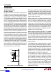
Figure 1 shows a simplified diagram of the four power
switches and their connections to the IC, inductor, V
IN
,
V
OUT
, ground, and current sense elements.
Figure 1. Converter Switch Diagram
Reverse current protection is accomplished through dis-
abling the V
OUT
side synchronous switch (D) during initial
power-up, when the converter is in step-up duty cycle
limit, and when ITH falls to a voltage that corresponds
to <1/25 of programmed I
LMAX
. Once these conditions
subside, the D switch remains disabled for an additional
128 clock cycles.
Figure 2. Operating Regions vs Duty Cycle (DC)
A
B
V
OUT
V
IN
R
SENSEB
TG2
SW2SW1
BG2
TG1
BG1
SENSEBOT
SENSETOP
D
B
*
*OPTIONAL
D
D
*
D
C
4020 F01
R
SENSEA
DC MAX
(BOOST)
DC MAX
(BUCK)
DC MIN
(BOOST)
DC MIN
(BUCK)
4020 F02
C/D PWM – A MIN OFF, B MIN ON
4-SWITCH PWM
A/B PWM – C MIN ON, D MIN OFF
Downloaded from Arrow.com.Downloaded from Arrow.com.Downloaded from Arrow.com.Downloaded from Arrow.com.Downloaded from Arrow.com.Downloaded from Arrow.com.Downloaded from Arrow.com.Downloaded from Arrow.com.Downloaded from Arrow.com.Downloaded from Arrow.com.Downloaded from Arrow.com.Downloaded from Arrow.com.Downloaded from Arrow.com.Downloaded from Arrow.com.Downloaded from Arrow.com.Downloaded from Arrow.com.Downloaded from Arrow.com.