
Datasheet


LTC4020
21
4020fd
For more information www.linear.com/LTC4020
DC/DC CONVERTER SECTION
Output Voltage Programming
The LTC4020 DC/DC converter maximum output volt
-
age, or voltage safety limit, is set by an external feedback
resistive divider, providing feedback to the V
FBMAX
pin.
This divider sets the output voltage that the converter
will servo to when the PowerPath FET is high impedance,
which occurs after charge cycle termination or during a
charge cycle fault.
applicaTions inForMaTion
PGND. Both nodes on the sense resistor must be Kelvin
connected to the IC, via the pins SENSBOT and SENSGND.
Both of these sense resistors must be of equal value, and
that value programs the switched inductor maximum
average current in the DC/DC converter inductor (I
LMAX
)
such that:
R
SENSEA
=R
SENSEB
=
0.05
I
LMAX
When the converter is stepping down, or operating in buck
mode, the inductor current will be roughly equivalent to
the converter output current. Input supply current (I
IN
) will
be less than the inductor current (I
L
), such that:
I
L
~I
IN
•
V
IN
V
OUT
When the converter is stepping up, or operating in boost
mode, the inductor current will be roughly equivalent to
the converter input current. Inductor current (I
L
) will be
greater than output current (I
OUT
), such that:
I
L
~I
OUT
•
V
OUT
V
IN
Overcurrent Detection
The LTC4020 also contains an overcurrent detection
circuit that monitors the low side current sense resistor,
or SENSBOT–SENSGND input. Should that circuit detect
a voltage on that input that is less than –150mV or greater
than 100mV, or roughly 3x the maximum average current,
all of the switches are disabled for four (4) clock cycles.
Parasitic inductances on non-ideal layouts and or body-
diode commutation charge can cause voltage spikes
across the sense resistor at the beginning of synchronous
FET conduction. The LTC4020 overcurrent circuitry is
somewhat resistant to these leading edge spikes but, in
some cases, the overcurrent circuit can be prematurely
triggered. This is identified by the repeated 4-cycle
switch off-time that occurs should premature triggering
occur. Placing a ceramic capacitor across the SENSBOT–
SENSGND input pins near the IC will generally eliminate
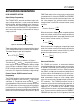
Figure 4. V
OUT
Safety Limit Programming
The resultant feedback signal is compared with the internal
2.75V voltage reference by the converter error amplifier.
The output voltage is given by the equation:
V
OUT
= 2.75V • 1+
R
MAX1
R
MAX2
where R
MAX1
and R
MAX2
are defined as in Figure 4.
The values for R
MAX1
and R
MAX2
are typically the same as
those used for the divider that programs battery voltage
(to the VFB pin; see Battery Charger section), to yield a
DC/DC converter maximum regulation voltage, or safety
limit, that is 10% higher than the battery charge voltage.
R
SENSEA
, R
SENSEB
: DC/DC Converter Current
Programming
The LTC4020 performs inductor current sensing via two
resistors connected in series with the V
IN
side switches
(see Figure 1). The high side sense resistor (R
SENSEA
) is
connected between V
IN
and the drain of the top side switch
FET (A). Both nodes on the sense resistor must be Kelvin
connected to the IC via the pins SENSVIN and SENSTOP.
Likewise, the low side sense resistor (R
SENSEB
) is connected
between the source of the bottom side switch FET (B) and
4020 F04
V
OUT
R
MAX1
R
MAX2
V
FBMAX
LTC4020
Downloaded from Arrow.com.Downloaded from Arrow.com.Downloaded from Arrow.com.Downloaded from Arrow.com.Downloaded from Arrow.com.Downloaded from Arrow.com.Downloaded from Arrow.com.Downloaded from Arrow.com.Downloaded from Arrow.com.Downloaded from Arrow.com.Downloaded from Arrow.com.Downloaded from Arrow.com.Downloaded from Arrow.com.Downloaded from Arrow.com.Downloaded from Arrow.com.Downloaded from Arrow.com.Downloaded from Arrow.com.Downloaded from Arrow.com.Downloaded from Arrow.com.Downloaded from Arrow.com.Downloaded from Arrow.com.