
Datasheet


LTC4020
22
4020fd
For more information www.linear.com/LTC4020
premature triggering by high pass filtering the current sense
signal. Setting the τ of the effective filter in the range of
1ns is generally sufficient to shunt errant signals, such that:
C
SENSB
~
1ns
R
SENSEB
Programming Switching Frequency
The RT frequency adjust pin allows the user to program
the LTC4020 DC/DC converter operating frequency from
50KHz to 500KHz.
Higher frequency operation is desirable for smaller ex
-
ternal inductor and capacitor values, but at the expense
of increased switching losses and higher gate drive cur-
rents. Higher frequencies may also not allow sufficiently
high or low duty cycle operation due to minimum on
/off
time
constraints. Lower operating frequencies require
larger external component values, but result in reduced
switching losses yielding higher conversion efficiencies.
Operating frequency (f
O
) is set by choosing an appropriate
frequency setting resistor (R
RT
), connected from the RT
pin to ground. This resistor is required for operation; do
not leave this pin open. For a desired operating frequency,
R
RT
follows the relation:
R
RT
=100kΩ •
f
O
250kHz
– 1.0695
Input Supply Decoupling
The LTC4020 is typically biased directly from the charger
input supply through the PV
IN
and SENSVIN pins. This
supply provides large switched currents, so a high quality,
low ESR decoupling capacitor is recommended to mini
-
mize voltage glitches on the V
IN
supply. Placing a smaller
ceramic capacitor (0.1µF to 10µF) close to the IC in parallel
with the input decoupling capacitor is also recommended
for high frequency noise reduction. The SENSVIN pin is a
Kelvin connection from the V
IN
supply at the primary V
IN
side switch FET (A); separate decoupling for that pin is
not recommended. The charger input supply decoupling
capacitor (C
VIN
) absorbs all input switching ripple current
in the charger, so it must have an adequate ripple current
rating. RMS ripple current (I
CVIN(RMS)
) is highest during
step down operation, and follows the relation:
I
CVIN(RMS)
~I
MAX
•DC•
1
DC
–
1
,
which has a maximum at DC = 0.5, or V
IN
= 2 • V
OUT
, where:
I
CVIN(RMS)
=
I
MAX
2
The simple worst-case of ½ • I
MAX
is commonly used for
design, where I
MAX
is the programmed inductor current
limit.
Bulk capacitance (C
IN(BULK)
) is a function of desired input
ripple voltage (ΔV
IN
). For step-down operation, C
IN(BULK)
follows the relation:
C
IN(BULK)
≥I
MAX
•
V
OUT(MAX)
V
IN(MIN)
•
1
ΔV
IN
• f
O
,
where f
O
is the operating frequency, V
OUT(MAX)
is the DC/
DC converter maximum output voltage and V
IN(MIN)
is
the regulation voltage corresponding to 2.5V on V
IN_REG
.
If the input regulation feature is not being used, use the
minimum expected input operating voltage.
If an application does not require step-down operation,
during step-up operation, input ripple current is equivalent
to inductor ripple current (ΔI
MAX
), so C
IN(BULK)
follows
the relation:
C
IN(BULK)
=
ΔI
MAX
ΔV
IN
• f
O
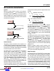
Figure 5. RT vs Operating Frequency
applicaTions inForMaTion
RT (kΩ)
50
OPERATING FREQUENCY (kHz)
600
500
400
300
200
100
0
250150 350 400 450
4020 F05
500200100 300
Downloaded from Arrow.com.Downloaded from Arrow.com.Downloaded from Arrow.com.Downloaded from Arrow.com.Downloaded from Arrow.com.Downloaded from Arrow.com.Downloaded from Arrow.com.Downloaded from Arrow.com.Downloaded from Arrow.com.Downloaded from Arrow.com.Downloaded from Arrow.com.Downloaded from Arrow.com.Downloaded from Arrow.com.Downloaded from Arrow.com.Downloaded from Arrow.com.Downloaded from Arrow.com.Downloaded from Arrow.com.Downloaded from Arrow.com.Downloaded from Arrow.com.Downloaded from Arrow.com.Downloaded from Arrow.com.Downloaded from Arrow.com.