
Datasheet


LTC4020
24
4020fd
For more information www.linear.com/LTC4020
the converter ripple current, so it must have an adequate
ripple current rating. RMS ripple current (I
ΔRMS
) is highest
during step up operation, and follows the relation:
I
ΔRMS
~I
MAX
•DC•
1
DC
–1
,
having a maximum at DC = 0.5, or V
OUT
= 2 • V
IN
, where:
I
CVOUT(RMS)
=
I
MAX
2
.
The simple worst-case of ½ • I
MAX
is commonly used for
design, where I
MAX
is the programmed inductor current
limit.
Bulk capacitance is a function of desired output ripple
voltage (ΔV
OUT
), and follows the relations:
For step-up operation:
C
OUT(BULK)
≥I
MAX
•
V
OUT(MAX)
– V
IN(MIN)
V
OUT(MAX)
•
1
ΔV
OUT
• f
O
,
where V
OUT(MAX)
is the DC/DC converter safety limit, and
V
IN(MIN)
is the V
IN
regulation threshold. If the V
IN
regula-
tion feature is not being used, use the minimum expected
operating voltage.
For step-down operation
, output ripple current is equivalent
to inductor ripple current (ΔI
MAX
), so C
OUT(BULK)
follows
the relation:
C
OUT(BULK)
≥
ΔI
MAX
ΔV
OUT
• f
O
,
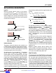
Switch FET Selection
The LTC4020 requires four external N-channel power
MOSFETs, as shown in Figure 1.
Specified parameters used for power MOSFET selection
are: breakdown voltage (V
BR(DSS)
), threshold voltage
(V
GS(TH)
), on-resistance (R
DS(ON)
), reverse transfer ca-
pacitance (C
RSS
), and maximum inductor current (I
LMAX
).
The drive voltage is set by the INTV
CC
supply pin, which is
typically 5V. Consequently, logic-level threshold MOSFETs
must be used in LTC4020 applications.
Transition Losses (P
TR
): During maximum power opera-
tion, all 4 switches change state once per oscillator cycle,
so the maximum switching transient power losses (P
TR
)
remain constant over condition.
P
TR(A, B)
≈ (k)(V
IN
)
2
(I
LMAX
)(C
RSS
)(f
O
)
P
TR(C, D)
≈ (k)(V
OUT
)
2
(I
LMAX
)(C
RSS
)(f
O
)
P
TR(A, B)
is the transition loss for the V
IN
side switch FETs
A and B, and P
TR(C,D)
is the transition loss for V
OUT
side
switch FETs C and D, with the switch FETs designated as
in Figure 1. The constant k, which accounts for the loss
caused by reverse recovery current, is inversely propor-
tional to the gate drive current and has a empirical value
approximated by k = 1 in LTC4020 applications. I
LMAX
is
the converter maximum inductor current as programmed
by the two sense resistors.
Conductive Losses (P
ON
): Conductive losses are propor-
tional to switch duty cycle. The average conductive losses
in a switch at maximum inductor current (I
LMAX
)is:
P
ON
= I
LMAX
2
• ρT • R
DS(ON)
• (T
ON
• f
O
)
where ρT is a normalization factor (unity at 25°C) ac-
counting for the significant variation in on-resistance
with temperature
.
For a maximum junction temperature
of 125°C, using a value of ρT = 1.5 is reasonable.
If V
IN
> V
OUT
(step-down conversion):
P
ON(A)
= I
LMAX
2
• ρT • R
DS(ON(A))
• (V
OUT
/V
IN
)
P
ON(B)
= I
LMAX
2
• ρT • R
DS(ON(B))
• (1 – V
OUT
/V
IN
)
P
ON(C+D)
= I
LMAX
2
• ρT • R
DS(ON(C, D))
If V
IN
< V
OUT
(step-up conversion):
P
ON(A+B)
= I
LMAX
2
• ρT • R
DS(ON(A, B))
P
ON(C)
= I
LMAX
2
• ρT • R
DS(ON(C))
• (1 – V
IN
/V
OUT
)
P
ON(D)
= I
LMAX
2
• ρT • R
DS(ON(D))
• (V
IN
/V
OUT
)
Optional Schottky Diode (Db, Dd) Selection
Schottky diodes can be placed in parallel with the syn-
chronous FETs B and D, as shown in Figure 1 as Db and
Dd.
These diodes conduct during the dead time between
the conduction of the power MOSFET switches and are
intended to prevent the body diode of synchronous switches
from storing charge.
applicaTions inForMaTion
Downloaded from Arrow.com.Downloaded from Arrow.com.Downloaded from Arrow.com.Downloaded from Arrow.com.Downloaded from Arrow.com.Downloaded from Arrow.com.Downloaded from Arrow.com.Downloaded from Arrow.com.Downloaded from Arrow.com.Downloaded from Arrow.com.Downloaded from Arrow.com.Downloaded from Arrow.com.Downloaded from Arrow.com.Downloaded from Arrow.com.Downloaded from Arrow.com.Downloaded from Arrow.com.Downloaded from Arrow.com.Downloaded from Arrow.com.Downloaded from Arrow.com.Downloaded from Arrow.com.Downloaded from Arrow.com.Downloaded from Arrow.com.Downloaded from Arrow.com.Downloaded from Arrow.com.