
Datasheet


LTC4020
26
4020fd
For more information www.linear.com/LTC4020
Figure 9. Connection of External 5V Regulator for Reduced
Internal Power Dissipation
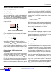
Figure 8. INTV
CC
Pass Element SOA (Safe Operating Area)
Q
G(TOT)ABCD
• f
O
(mA)
0
V
IN
(V)
60
50
40
30
20
10
0
4020 60 70 80
4020 F08
903010 50
SOA
4020 F09
LTC4020
V
IN
SENSVIN
INTV
CC
V
IN
V
IN
(5V)
5V
OUT
or large gate drive requirements. The power dissipation
in the linear pass element (P
INTVCC
) is:
P
INTVCC
= (V
IN
– 5V) • Q
G(TOT)ABCD
• f
O
,
where Q
G(TOT)ABCD
is the sum of all four switch total gate
charges, and f
O
is the LTC4020 switching frequency.
In this configuration, the INTV
CC
pin cannot collapse
when the LTC4020 is in shutdown. As a result of the pin
bias being maintained during shutdown, current will flow
into the INTV
CC
pin, increasing input supply current. The
total shutdown current flowing into the INTV
CC
pin in this
configuration is approximately 150µA.
BATTERY CHARGER SECTION
Battery Charge Voltage Programming
The LTC4020 uses an external feedback resistive divider
from the BAT pin to ground to program battery voltages.
This divider provides feedback to the VFB pin, and sets
the final voltage that the battery charger will achieve at
the end of a charge cycle. The feedback reference of 2.5V
corresponds to the battery float voltage during CC/CV
mode charging (MODE = 0V).
applicaTions inForMaTion
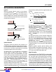
Figure 11. Battery Voltage Programming
Figure 10. Connection of Low-Voltage Input Supply
If desired operation places the internal 5V regulator out
of the allowable SOA region, deriving gate drive power
externally is required.
For driving the LTC4020 with an external 5V regulator,
connect the PV
IN
and INTV
CC
pins to that regulator output
as shown in Figure 9. The SENSVIN pin remains connected
to the input supply.
4020 F10
LTC4020
V
IN
SENSVIN
INTV
CC
V
IN
(4.5V TO 5.5V)
4020 F11
R
FB1
(BATTERY)
R
FB2
VFB
VBAT
LTC4020
For operation with tightly regulated low voltage input sup-
plies (4.5V to
5.5V), the LTC4020 internal gate drivers and
BST refresh functions can be powered directly by the input
supply, eliminating the requirement for a 5V regulator to
supply the INTV
CC
pin. Connect the input supply to the
PV
IN
, INTV
CC
, and SENSVIN pins, as shown in Figure 10.
The resultant feedback signal is compared with the internal
2.5V voltage reference by the converter error amplifier.
The output voltage is given by the equation:
V
(FLOAT(CC/CV)
= 2.5V 1+
R
FB1
R
FB2
where R
FB1
and R
FB2
are defined as in Figure 11.
If charging in CC mode (MODE = -NC-), R
FB1
and R
FB2
corresponding to V
FB
= 2.5V programs a maximum V
BAT
voltage, if constant-voltage functionality at that level if
desired.
Downloaded from Arrow.com.Downloaded from Arrow.com.Downloaded from Arrow.com.Downloaded from Arrow.com.Downloaded from Arrow.com.Downloaded from Arrow.com.Downloaded from Arrow.com.Downloaded from Arrow.com.Downloaded from Arrow.com.Downloaded from Arrow.com.Downloaded from Arrow.com.Downloaded from Arrow.com.Downloaded from Arrow.com.Downloaded from Arrow.com.Downloaded from Arrow.com.Downloaded from Arrow.com.Downloaded from Arrow.com.Downloaded from Arrow.com.Downloaded from Arrow.com.Downloaded from Arrow.com.Downloaded from Arrow.com.Downloaded from Arrow.com.Downloaded from Arrow.com.Downloaded from Arrow.com.Downloaded from Arrow.com.Downloaded from Arrow.com.