
Datasheet


LTC4020
28
4020fd
For more information www.linear.com/LTC4020
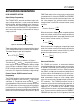
Figure 13. V
OUT
Instant-On Programming
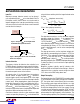
Figure 14. Instant-On Charger Current Sense Limit Reduction
The resultant feedback signal is compared with the internal
2.125V voltage reference by a dedicated instant-on error
amplifier, the output of which servos the BGATE pin. The
output voltage is given by the equation:
V
OUT
= 2.125V 1+
R
MIN1
R
MIN2
where R
MIN1
and R
MIN2
are defined as in Figure 13.
When the DC/DC converter is operating, but the battery
charger is not in a charging cycle, the PowerPath FET is
automatically configured as an ideal diode between the BAT
pin (anode) and the CSN pin (cathode). The ideal diode
function allows the battery to remain disconnected from the
converter output while the converter is supplying power,
but also allows the battery to be efficiently engaged for ad
-
ditional power should a load exceed the DC/DC converter’s
capability. This ideal diode circuit regulates the external
FET to achieve low loss conduction, maintaining a voltage
drop of 14mV across from the BAT pin to the CSN pin,
provided the battery current load though the ideal diode
does not exceed 14mV/R
DS(ON)
. With larger currents, the
FET will behave like a fixed value resistor equal to R
DS(ON)
.
In certain applications, the PowerPath function is not
required. For example, lead-acid chargers do not termi
-
nate (they remain in float charging mode indefinitely),
so the battery need never be disconnected from the
output, provided the instant-on feature is not desired.
The PowerPath FET can be eliminated in these applica-
tions by tying the CSN side of the sense resistor to BAT,
connecting V
FBMIN
to ground, and connecting a 100pF
capacitor from the BGATE pin to CSN. See Typical Ap-
plication Circuits section.
RNG
/SS: Dynamic Current Limit Adjust
Maximum charge current can be dynamically adjusted
using the RNG
/SS pin as described in the Pin Description
section. Active servos can also be used to impose voltages
on the RNG/SS pin, provided they can only sink current.
Active circuits that source current cannot be used to drive
the RNG/SS pin.
applicaTions inForMaTion
Figure 15. Using the RNG/SS Pin for Digital Control of
Maximum Charge Current
4020 F15
10k
LOGIC HIGH = HALF CURRENT
RNG/SS
LTC4020
4020 F13
V
OUT
R
MIN1
R
MIN2
V
FBMIN
LTC4020
The values for R
MIN1
and R
MIN2
are typically the same as
those used for the divider that programs battery voltage
(to the VFB pin; see Battery Charger section), to yield a
DC/DC converter minimum operational regulation voltage
corresponding to 85% of the battery charge voltage.
During instant-on operation, if the drain-to-source voltage
across the PowerPath FET (V
CSN
– V
BAT
) exceeds 0.45V,
the maximum charge current is automatically reduced.
Maximum charge current is reduced linearly across the
range of 0.45V < V
CSN
– V
BAT
< 1.95V to one-fifteenth of
the current programmed by the battery charger sense
resistor, RCS. This reduction in charge current helps to
prevent excessive power dissipation in the PowerPath FET.
V
CSN–BAT
(V)
0
MAXIMUM CHARGE CURRENT (%)
100
90
70
50
80
60
40
30
20
10
0
0.5 1 1.25
4020 F14
2.251.5 1.75 2.520.25 0.75
Downloaded from Arrow.com.Downloaded from Arrow.com.Downloaded from Arrow.com.Downloaded from Arrow.com.Downloaded from Arrow.com.Downloaded from Arrow.com.Downloaded from Arrow.com.Downloaded from Arrow.com.Downloaded from Arrow.com.Downloaded from Arrow.com.Downloaded from Arrow.com.Downloaded from Arrow.com.Downloaded from Arrow.com.Downloaded from Arrow.com.Downloaded from Arrow.com.Downloaded from Arrow.com.Downloaded from Arrow.com.Downloaded from Arrow.com.Downloaded from Arrow.com.Downloaded from Arrow.com.Downloaded from Arrow.com.Downloaded from Arrow.com.Downloaded from Arrow.com.Downloaded from Arrow.com.Downloaded from Arrow.com.Downloaded from Arrow.com.Downloaded from Arrow.com.Downloaded from Arrow.com.