
Datasheet
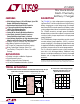


LTC4020
5
4020fd
For more information www.linear.com/LTC4020
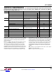
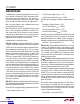
SYMBOL PARAMETER CONDITIONS MIN TYP MAX UNITS
BGATE BGATE Pull-Down Current Charging Enabled 15 µA
BGATE Pull-Up Current Charging Disabled; V
CSN
– V
BGATE
= 2V 15 µA
BGATE Standby Pull-Down Current V
SHDN
= 0V 120 µA
Ideal Diode Pull-Down Current Charging Disabled; V
BAT
– V
CSN
= 0.5V 500 µA
Ideal Diode Forward Voltage V
BAT
– V
CSN
; V
CSN
Measured Through
100Ω Series Resistor
l
5 14 20 mV
TIMER Timer High Threshold 1.5 V
Timer Low Threshold 1.0 V
C/10 Mode Threshold (Rising)
l
0.4 0.5 0.6 V
C/10 Mode Hysteresis 225 mV
Timer Source/Sink Current V
TIMER
= 1.25V
l
8.5 10 11.5 µA
V
STAT(L)
Status Pins Enabled Voltage I
STAT1
= 1mA; I
STAT2
= 1mA
I
STAT1
= 5mA; I
STAT2
= 5mA
l
l
0.15
0.75
0.4
2.5
V
V
I
VFBMIN
Instant-On Feedback Bias Current 10 nA
I
VFB
Feedback Pin Bias Current 10 nA
I
VIN_REG
Input Regulation Bias Current 10 nA
I
FBG
Pin Current (Disabled) V
SHDN
= 0V; V
FBG
= 55V 10 nA
R
NTC
NTC Minimum Disable Resistance
l
250 400 kΩ
R
FBG
FBG Resistance to SGND I
FBG
= 1mA
l
20 50 Ω
elecTrical characTerisTics
The l denotes the specifications which apply over the specified operating
junction temperature range, otherwise specifications are at T
A
= 25°C (Note 2). PV
IN
= SENSVIN = CSP = CSN = BAT = 20V, SHDN = 2V,
C
(TG1, BG1, TG2, BG2)
= 1000pF, V
RNG/SS
= 2V.
Note 1: Stresses beyond those listed under Absolute Maximum Ratings
may cause permanent damage to the device. Exposure to any Absolute
Maximum Rating condition for extended periods may affect device
reliability and lifetime.
Note 2: The LTC4020 is tested under pulsed load conditions such that
T
J
≈ T
A
. The LTC4020E is guaranteed to meet specifications from
0°C to 85°C junction temperature. Specifications over the –40°C to
125°C operating junction temperature range are assured by design,
characterization, and correlation with statistical process controls. The
LTC4020I is guaranteed over the full –40°C to 125°C operating junction
temperature range. The junction temperature (T
J
) is calculated from
the ambient temperature (T
A
) and power dissipation (PD) according
to the formula T
J
= T
A
+ (PD • θJ
A
). Note that the maximum ambient
temperature consistent with these specifications is determined by specific
operating conditions in conjunction with board layout, the rated package
thermal resistance and other environmental factors. This IC includes
overtemperature protection that is intended to protect the device during
momentary overload. Junction temperature will exceed 125°C when
overtemperature protection is active. Continuous operation above the
specified maximum operating junction temperature may impair device
reliability.
Note 3:
ICC does not include switching currents. V
BST1
= V
BST2
= V
INTVCC
and V
SW1
= V
SW2
= 0V for testing.
Note 4: See Typical Performance Characteristics
Downloaded from Arrow.com.Downloaded from Arrow.com.Downloaded from Arrow.com.Downloaded from Arrow.com.Downloaded from Arrow.com.