
Datasheet


LTC4098/LTC4098-1
26
40981fc
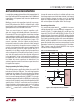
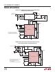
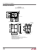
Figure 10. Ground Currents Follow Their Incident Path
at High Speed. Slices in the Ground Plane Cause High
Voltage and Increased Emissions
40981 F10
APPLICATIONS INFORMATION
USB Inrush Limiting
The USB specification allows at most 10μF of downstream
capacitance to be hot-plugged into a USB hub. In most
LTC4098/LTC4098-1 applications, 10μF should be enough
to provide adequate filtering on V
BUS
.
If more capacitance is required, the OVP circuit will provide
adequate soft-connect time to prevent excessive inrush
currents. An additional 22μF on the V
BUS
pin will gener-
ally contribute less than 100mA to the hot-plug inrush
current.
Voltage overshoot on V
BUS
may sometimes be observed
when connecting the LTC4098/LTC4098-1 to a lab power
supply. This overshoot is caused by long leads from the
power supply to V
BUS
. Twisting the wires together from
the supply to V
BUS
can greatly reduce the parasitic induc-
tance of these long leads, and keep the voltage at V
BUS
to
safe levels. USB cables are generally manufactured with
the power leads in close proximity, and thus fairly low
parasitic inductance.
Board Layout Considerations
The Exposed Pad on the backside of the LTC4098/
LTC4098-1 package must be securely soldered to the PC
board ground. This is the primary ground pin in the pack-
age, and it serves as the return path for both the control
circuitry and the synchronous rectifier.
Furthermore, due to its high frequency switching circuitry,
it is imperative that the input capacitor, inductor, and
output capacitor be as close to the LTC4098/LTC4098-1
as possible and that there be an unbroken ground plane
under the LTC4098/LTC4098-1 and all of its external high
frequency components. High frequency currents, such as
the input current on the LTC4098/LTC4098-1, tend to find
their way on the ground plane along a mirror path directly
beneath the incident path on the top of the board. If there
are slits or cuts in the ground plane due to other traces
on that layer, the current will be forced to go around the
slits. If high frequency currents are not allowed to flow
back through their natural least-area path, excessive
voltage will build up and radiated emissions will occur
(see Figure 10). There should be a group of vias directly
under the grounded backside leading directly down to an
internal ground plane. To minimize parasitic inductance,
the ground plane should be as close as possible to the
top plane of the PC board (layer 2).
The IDGATE pin for the external ideal diode controller has
extremely limited drive current. Care must be taken to
minimize leakage to adjacent PC board traces. 100nA of
leakage from this pin will introduce an additional offset to
the ideal diode of approximately 10mV. To minimize leakage,
the trace can be guarded on the PC board by surrounding
it with V
OUT
connected metal, which should generally be
less than one volt higher than IDGATE.