
Datasheet

LTC4227
16
422712fa
For more information www.linear.com/LTC4227
applicaTions inForMaTion
For C
L
= 680µF, the time it takes to charge up C
L
is cal-
culated as:
t
CHARGE
=
C
L
• V
IN
I
INRUSH
=
680µF •12V
0.5A
= 16ms
The inrush current is set to 0.5A by adding capacitance,
C
HG
, at the gate of the Hot Swap MOSFET.
C
HG
=
C
L
• I
HGATE(UP)
I
INRUSH
=
680µF • 10µA
0.5A
≅ 15nF
The average power dissipated in the MOSFET is calculated
as:
P
AVG
=
E
CL
t
CHARGE
=
1
2
•
680µF • 12V
( )
2
16ms
= 3W
The MOSFET selected must be able to tolerate 3W for
16ms during power-up. The SOA curves of the Si7336ADP
provide for 1.5A at 30V (45W) for 100ms. This is suffi
-
cient to satisfy the requirement. The increase in junction
temperature due to the power dissipated in the MOSFET
is ∆T = P
AVG
• Zth
JC
where Zth
JC
is the junction-to-case
thermal impedance. Under this condition, the Si7336ADP
data sheet indicates that the junction temperature will
increase by 2.4°C using Zth
JC
= 0.8°C/W (single pulse).
The duration and magnitude of the power pulse during
an output short is a function of the TMR capacitance, C
T
,
and the LTC4227’s active current limit. The short-circuit
duration is given as C
T
• 12[ms/µF] = 1.2ms for C
T
= 0.1µF.
The maximum short-circuit current is calculated using the
maximum active current limit threshold, ∆V
SENSE(ACL)(MAX)
and minimum R
S
value.
I
SHORT(MAX)
=
∆V
SENSE(ACL)(MAX)
R
S(MIN)
=
70mV
5.94mΩ
= 11.8A
So, the maximum power dissipated in the MOSFET is
11.8A • 12V = 142W for 1.2ms. The Si7336ADP data
sheet indicates that the worst-case increase in junc
-
tion temperature during this short-circuit condition is
21.3°C using Zth
JC
= 0.15°C/W (single pulse). Choosing
C
T
= 0.1µF will not cause the maximum junction tempera-
ture of the MOSFET to be exceeded. The SOA curves of
the Si7336ADP provide for 6A at 30V (180W) for 10ms.
This also satisfies the requirement.
Next, select the resistive divider at the ON pin to provide
an undervoltage threshold of 9.6V for the 12V supply at
SENSE
+
. First, choose the bottom resistor, R1, to be 20k.
Then, calculate the top resistor value for R2:
R2 =
V
IN(UVTH)
V
ON(TH)
– 1
• R1
R2 =
9.6V
1.235V
– 1
• 20k = 135k
Choose the nearest 1% resistor value of 137k for R2. In
addition, there is a 0.1µF bypass, C1, at the INTV
CC
pin
and a 10nF filter capacitor, C
F
, at the ON pin to prevent the
supply glitches from turning off the Hot Swap MOSFET.
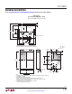
PCB Layout Considerations
For proper operation of the LTC4227’s circuit breaker,
Kelvin connection to the sense resistor is strongly rec
-
ommended. The PCB layout should be balanced and
symmetrical to minimize wiring errors. In addition, the
PCB layout for the sense resistor and the power MOSFET
should include good thermal management techniques for
optimal device power dissipation. A recommended PCB
layout is illustrated in Figure 7.
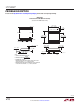
Connect the IN and OUT pin traces as close as possible to
the MOSFET s’ terminals. Keep the traces to the MOSFETs
wide and short to minimize resistive losses. The PCB traces
associated with the power path through the MOSFETs
should have low resistance. The suggested trace width for
1oz copper foil is 0.03" for each ampere of DC current to
keep PCB trace resistance, voltage drop and temperature
rise to a minimum. Note that the sheet resistance of 1oz
copper foil is approximately 0.5mΩ/square, and voltage
drops due to trace resistance add up quickly in high cur
-
rent applications.
It is also important to place the bypass capacitor, C1, for