
Datasheet


LTC4252-1/LTC4252-2
LTC4252A-1/LTC4252A-2
16
425212fe
For more information www.linear.com/LTC4252-1
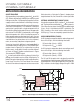
applicaTions inForMaTion
conditions are met. A high-to-low transition in the UV
comparator immediately shuts down the LTC4252, pulls
the MOSFET gate low and resets the latched PWRGD high.
Overvoltage conditions detected by the OV compara
-
tor will also pull GATE low, thereby shutting down the
load. However, it will not reset the cir
cuit breaker TIMER,
PWRGD flag or shutdown cooling timer. Returning the
supply voltage to an acceptable range restarts the GATE
pin if all the interlock conditions except TIMER are met.
Only during the initial timing cycle does an OV condition
reset the TIMER.
DRAIN
Connecting an external resistor, R
D
, to the dual function
DRAIN pin allows V
OUT
sensing* without it being dam-
aged by large voltage transients. Below 5V, negligible pin
leakage allows a DRAIN low comparator to detect V
OUT
less than 2.385V (V
DRNL
). This condition, together with
the GATE low comparator, sets the PWRGD flag.
If V
OUT
> V
DRNCL
, the DRAIN pin is clamped at about
V
DRNCL
and the current flowing in R
D
is given by:
I
DRN
≈
V
OUT
-V
DRNCL
R
D
(1)
This current is scaled up 8 times during a circuit breaker
fault and is added to the nominal 230µA TIMER current.
This accelerates the fault TIMER pull-up when the MOS
-
FET’s drain-source voltage exceeds V
DRNCL
and effectively
shortens the MOSFET heating duration.
TIMER
The operation of the TIMER pin is somewhat complex as
it handles several key functions. A capacitor C
T
is used at
TIMER to provide timing for the LTC4252. Four different
charging and discharging modes are available at TIMER:
1) A 5.8µA slow charge; initial timing and shutdown cool
-
ing delay.
2) A
(230µA + 8 • I
DRN
) fast charge; circuit breaker delay.
3) A 5.8µA slow discharge; circuit breaker “cool off” and
shutdown cooling.
4) Low impedance switch; resets the TIMER capacitor
after an initial timing delay, in UVLO, in UV and in OV
during initial timing.
For initial start-up, the 5.8µA pull-up is used. The low
impedance switch is turned off and the 5.8µA current
source is enabled when the interlock conditions are met.
C
T
charges to 4V in a time period given by:
t=
4V •C
T
5.8µA
(2)
When C
T
reaches 4V (V
TMRH
), the low impedance switch
turns on and discharges C
T
. A GATE start-up cycle begins
and both SS and GATE are released.
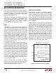
CIRCUIT BREAKER TIMER OPERATION
If the SENSE pin detects more than a 50mV drop across
R
S
, the TIMER pin charges C
T
with (230µA + 8 • I
DRN
). If
C
T
charges to 4V, the GATE pin pulls low and the LTC4252-1
latches off while the LTC4252-2 starts a shutdown cooling
cycle. The LTC4252-1 remains latched off until the UV
pin is momentarily pulsed low or TIMER is momentarily
discharged low by an external switch or V
IN
dips below
UVLO and is then restored. The circuit breaker timeout
period is given by:
t=
4V •C
T
230µA+8•I
DRN
(3)
If V
OUT
< 5V, an internal PMOS device isolates any DRAIN
pin leakage current, making I
DRN
= 0µA in Equation (3).
If V
OUT
> V
DRNCL
during the circuit breaker fault period,
the charging of C
T
accelerates by 8 • I
DRN
of Equation (1).
Intermittent overloads may exceed the 50mV threshold at
SENSE, but, if their duration is sufficiently short, TIMER
will not reach 4V and the LTC4252 will not shut the external
MOSFET off. To handle this situation, the TIMER discharges
C
T
slowly with a 5.8µA pull-down whenever the SENSE
voltage is less than 50mV. Therefore, any intermittent
overload with V
OUT
> 5V and an aggregate duty cycle of
*V
OUT
as viewed by the MOSFET; i.e., V
DS
.