
Datasheet


LTC4252-1/LTC4252-2
LTC4252A-1/LTC4252A-2
20
425212fe
For more information www.linear.com/LTC4252-1
Approximating a linear charging rate as I
DRN
drops from
I
DRN(MAX)
to zero, the I
DRN
component in Equation (3)
can be approximated with 0.5 • I
DRN(MAX)
. Rearranging
equation, TIMER capacitor C
T
is given by:
C
T
=
t
CL(CHARGE)
• 230µA+4•I
DRN(MAX)
( )
4V
(13)
Returning to Equation (3), the TIMER period is calcu-
lated and used in conjunction with V
SUPPLY(MAX)
and
I
SHORTCIRCUIT(MAX)
to check the SOA curves of a prospec-
tive MOSFET.
As a numerical design example, consider a 30W load,
which requires 1A input current at 36V. If V
SUPPLY(MAX)
= 72V and C
L
= 100µF, R
D
= 1MΩ, Equation (8) gives R
S
= 40mΩ; Equation (13) gives C
T
= 441nF. To account for
errors in R
S
, C
T
, TIMER current (230µA), TIMER threshold
(4V), R
D
, DRAIN current multiplier and DRAIN voltage
clamp (V
DRNCL
), the calculated value should be multiplied
by 1.5, giving the nearest standard value of C
T
= 680nF.
If a short-circuit occurs, a current of up to 120mV/40mΩ=3A
will flow in the MOSFET for 5.6ms as dictated by C
T
=680nF
in Equation (3). The MOSFET must be selected based on
this criterion. The IRF530S can handle 100V and 3A for
10ms and is safe to use in this application.
Computing the maximum soft-start capacitor value during
soft-start to a load short is complicated by the nonlinear
MOSFET’s SOA characteristics and the R
SS
C
SS
response.
An overly conservative but simple approach begins with
the maximum circuit breaker current, given by:
I
CB(MAX)
=
V
CB(MAX)
R
S
(14)
where V
CB(MAX)
= 60mV (55mV for the LTC4252A).
From the SOA curves of a prospective MOSFET, determine
the time allowed, t
SOA(MAX)
. C
SS
is given by:
C
SS
=
t
SOA(MAX)
0.916 •R
SS
(15)
In the above example, 60mV/40mΩ gives 1.5A. t
SOA(MAX)
for the IRF530S is 40ms. From Equation (15), C
SS
=
437nF. Actual board evaluation showed that C
SS
= 100nF
was appropriate. The ratio (R
SS
• C
SS
) to t
CL(CHARGE)
is
a good gauge as a large ratio may result in the time-out
period expiring. This gauge is determined empirically with
board level evaluation.
SUMMARY OF DESIGN FLOW
To summarize the design flow, consider the application
shown in Figure 2 with the LTC4252A. It was designed
for 80W.
Calculate the maximum load current: 80W/43V = 1.86A;
allowing for 83% converter efficiency, I
IN(MAX)
= 2.2A.
Calculate R
S
: from Equation (8) R
S
= 20mΩ.
Calculate I
SHORTCIRCUIT(MAX)
: from Equation (10)
I
SHORTCIRCUIT(MAX)
=
66mV
20mΩ
=3.3A
Select a MOSFET that can handle 3.3A at 71V: IRF530S.
Calculate C
T
: from Equation (13) C
T
= 322nF. Select
C
T
=680nF, which gives the circuit breaker time-out period
t= 5.6ms.
Consult MOSFET SOA curves: the IRF530S can handle 3.3A
at 100V for 8.2ms, so it is safe to use in this application.
Calculate C
SS
: using Equations (14) and (15) select
C
SS
=68nF.
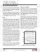
FREQUENCY COMPENSATION
The LTC4252A typical frequency compensation network for
the analog current limit loop is a series R
C
(10Ω) and C
C
connected to V
EE
. Figure 7 depicts the relationship between
the compensation capacitor C
C
and the MOSFET’s C
ISS
.
The line in Figure 7 is used to select a starting value for C
C
based upon the MOSFET’s C
ISS
specification. Optimized
values for C
C
are shown for several popular MOSFETs.
Differences in the optimized value of C
C
versus the starting
value are small. Nevertheless, compensation values should
be verified by board level short-circuit testing.
applicaTions inForMaTion