
Datasheet


LTC4252-1/LTC4252-2
LTC4252A-1/LTC4252A-2
21
425212fe
For more information www.linear.com/LTC4252-1
applicaTions inForMaTion
As seen in Figure 6 previously, at the onset of a short-
circuit event, the input supply voltage can ring dramatically
owing to series inductance. If this voltage avalanches the
MOSFET, current continues to flow through the MOSFET
to the output. The analog current limit loop cannot control
this current flow and therefore the loop undershoots. This
effect cannot be eliminated by frequency compensation. A
zener diode is required to clamp the input supply voltage
and prevent MOSFET avalanche.
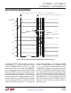
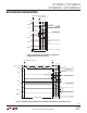
SENSE RESISTOR CONSIDERATIONS
For proper circuit breaker operation, Kelvin-sense PCB con
-
nections between the sense resistor and the LTC4252’s V
EE
and SENSE pins are strongly recommended. The drawing in
Figure 8 illustrates the correct way of making connections
between the LTC4252 and the sense resistor. PCB layout
should be balanced and symmetrical to minimize wiring
errors. In addition, the PCB layout for the sense resistor
should include good thermal management techniques for
optimal sense resistor power dissipation.
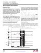
TIMING WAVEFORMS
System Power-Up
Figure 9 details the timing waveforms for a typical power-
up sequence in the case where a board is already installed
in the backplane and system power is applied abruptly. At
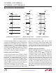
MOSFET C
ISS
(pF)
0
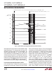
COMPENSATION CAPACITANCE C
C
(nF)
60
50
40
30
20
10
0
2000
4000
425212 F07
6000
8000
NTY100N10
IRF3710
IRF540S
IRF530S
IRF740
Figure 7. Recommended Compensation
Capacitor C
C
vs MOSFET C
ISS
Figure 8. Making PCB Connections to the Sense Resistor
W
CURRENT FLOW
FROM LOAD
CURRENT FLOW
TO –48V BACKPLANE
SENSE RESISTOR
TRACK WIDTH W:
0.03" PER AMP
ON 1 OZ COPPER
TO
SENSE
TO
V
EE
425212 F08
time point 1, the supply ramps up, together with UV/OV,
V
OUT
and DRAIN. V
IN
and PWRGD follow at a slower rate
as set by the V
IN
bypass capacitor. At time point 2, V
IN
exceeds V
LKO
and the internal logic checks for UV > V
UVHI
,
OV < V
OVLO
, GATE < V
GATEL
, SENSE < V
CB
, SS < 20 • V
OS
and TIMER < V
TMRL
. If all conditions are met, an initial
timing cycle starts and the TIMER capacitor is charged
by a 5.8µA current source pull-up. At time point 3, TIMER
reaches the V
TMRH
threshold and the initial timing cycle
terminates. The TIMER capacitor is quickly discharged. At
time point 4, the V
TMRL
threshold is reached and the condi-
tions of GATE < V
GATEL
, SENSE < V
CB
and SS<20•V
OS
must be satisfied before a GATE ramp-up cycle begins.
SS ramps up as dictated by R
SS
• C
SS
(as in Equation 6);
GATE is held low by the analog current limit (ACL) ampli-
fier until SS crosses 20 • V
OS
. Upon releasing GATE, 58µA
sources into the external MOSFET gate and compensation
network. When the GATE voltage reaches the MOSFET’s
threshold, current begins flowing into the load capacitor
at time point 5. At time point 6, load current reaches the
SS control level and the analog current limit loop activates.
Between time points 6 and 8, the GATE voltage is servoed,
the SENSE voltage is regulated at V
ACL
(t) (Equation 7) and
soft-start limits the slew rate of the load current. If the
SENSE voltage (V
SENSE
– V
EE
) reaches the V
CB
threshold
at time point 7, the circuit breaker TIMER activates. The
TIMER capacitor, C
T
, is charged by a (230µA + 8 • I
DRN
)
current pull-up. As the load capacitor nears full charge,
load current begins to decline.