
Datasheet


LTC4252-1/LTC4252-2
LTC4252A-1/LTC4252A-2
24
425212fe
For more information www.linear.com/LTC4252-1
applicaTions inForMaTion
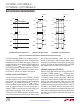
Undervoltage Timing
In Figure 11 when UV pin drops below V
UVLO
(time point1),
the LTC4252 shuts down with TIMER, SS and GATE all
pulling low. If current has been flowing, the SENSE pin
voltage decreases to zero as GATE collapses. When UV
recovers and clears V
UVHI
(time point 2), an initial timer
cycle begins followed by a GATE start-up cycle.
V
IN
Undervoltage Lockout Timing
The V
IN
undervoltage lockout comparator, UVLO, has a
similar timing behavior as the UV pin timing except it looks
for V
IN
< (V
LKO
– V
LKH
) to shut down and V
IN
> V
LKO
to
start. In an undervoltage lockout condition, both UV and
OV comparators are held off. When V
IN
exits undervoltage
lockout, the UV and OV comparators are enabled.
Undervoltage Timing with Overvoltage Glitch
In Figure 12, both UV and OV pins are connected together.
When UV clears V
UVHI
(time point 1), an initial timing
cycle starts. If the system bus voltage overshoots V
OVHI
as shown at time point 2, TIMER discharges. At time point
3, the supply voltage recovers and drops below the V
OVLO
threshold. The initial timing cycle restarts, followed by a
GATE start-up cycle.
Overvoltage Timing
During normal operation, if the OV pin exceeds V
OVHI
as
shown at time point 1 of Figure 13, the TIMER and PWRGD
status are unaffected. Nevertheless, SS and GATE pull down
and the load is disconnected. At time point 2, OV recovers
and drops below the V
OVLO
threshold. A GATE start-up
cycle begins. If the overvoltage glitch is long enough to
deplete the load capacitor, a full start-up cycle as shown
between time points 4 through 7 may occur.
Circuit Breaker Timing
In Figure 14a, the TIMER capacitor charges at 230µA if
the SENSE pin exceeds V
CB
but V
DRN
is less than 5V. If
the SENSE pin drops below V
CB
before TIMER reaches
UV
TIMER
GATE
SENSE
SS
DRAIN
PWRGD
5.8µA
58µA
5.8µA
5.8µA
58µA
UV DROPS BELOW V
UVLO
. GATE, SS AND TIMER ARE PULLED DOWN, PWRGD RELEASES
1 2 3 4 56 7 8 9
TIMER CLEARS V
TMRL
, CHECK GATE < V
GATEL
, SENSE < V
CB
AND SS < 20 • V
OS
10 11
425212 F11
UV CLEARS V
UVHI
, CHECK OV CONDITION, GATE < V
GATEL
, SENSE < V
CB
, SS < 20 • V
OS
AND TIMER < V
TMRL
V
ACL
V
CB
230µA + 8 • I
DRN
20 • V
OS
V
IN
– V
GATEH
V
DRNL
V
DRNCL
20 • (V
CB
+ V
OS
)
20 • (V
ACL
+ V
OS
)
V
GATEL
V
TMRL
V
TMRH
V
UVHI
V
UVLO
GATE
START-UP
INITIAL TIMING
Figure 11. Undervoltage Timing (All Waveforms Are Referenced to V
EE
)