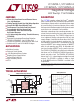
LTC4252-1/LTC4252-2 LTC4252A-1/LTC4252A-2 Negative Voltage Hot Swap Controllers Features n n n n n n n ■ ■ ■ ■ Description Allows Safe Board Insertion and Removal from a Live – 48V Backplane Floating Topology Permits Very High Voltage Operation Current Limit With Circuit Breaker Timer Fast Response Time Limits Peak Fault Current Programmable Soft-Start Current Limit Programmable Timer with Drain Voltage Accelerated Response ±1% Undervoltage/Overvoltage Threshold Accuracy (LTC4252A) Adjustable Undervolt
LTC4252-1/LTC4252-2 LTC4252A-1/LTC4252A-2 Absolute Maximum Ratings All Voltages Referred to VEE (Note 1) Current into VIN (100µs Pulse)..............................100mA VIN, DRAIN Pin Minimum Voltage......................... – 0.3V Input/Output Pins (Except SENSE and DRAIN) Voltage........... –0.3V to 16V SENSE Pin Voltage..................................... –0.6V to 16V Current Out of SENSE Pin (20µs Pulse) ........... –200mA Current into DRAIN Pin (100µs Pulse)....................
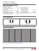
LTC4252-1/LTC4252-2 LTC4252A-1/LTC4252A-2 Electrical Characteristics The l denotes the specifications which apply over the full operating temperature range, otherwise specifications are at TA = 25°C. (Note 2) SYMBOL PARAMETER CONDITIONS VZ VIN – VEE Zener Voltage IIN = 2mA l LTC4252-1/-2 MIN TYP MAX LTC4252A-1/-2 MIN TYP MAX 11.5 11.5 13 14.5 14.5 V rZ VIN – VEE Zener Dynamic Impedance IIN = 2mA to 30mA VIN Supply Current UV = OV = 4V, VIN = (VZ – 0.3V) ● 0.8 2 0.
LTC4252-1/LTC4252-2 LTC4252A-1/LTC4252A-2 Electrical Characteristics The l denotes the specifications which apply over the full operating temperature range, otherwise specifications are at TA = 25°C. (Note 2) LTC4252-1/-2 MIN TYP MAX LTC4252A-1/-2 MIN TYP MAX Timer On (Initial Cycle/Latchoff/ Shutdown Cooling, Sourcing), VTMR = 2V 5.8 5.
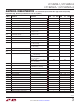
LTC4252-1/LTC4252-2 LTC4252A-1/LTC4252A-2 Typical Performance Characteristics 14.0 VZ vs Temperature 10 IIN = 2mA rZ vs Temperature 2000 IIN = 2mA TO 30mA 1800 9 13.5 1400 1200 IIN (µA) rZ (Ω) VZ (V) 7 6 1000 5 12.5 400 3 200 2 –55 –35 –15 5 25 45 65 85 105 125 TEMPERATURE (°C) 425212 G03 1.3 11.0 TA = 125°C VLKH (V) TA = 85°C 10.5 VLKO (V) IIN (mA) 1.5 11.5 TA = 25°C 1 Undervoltage Lockout Hysteresis VLKH vs Temperature 12.
LTC4252-1/LTC4252-2 LTC4252A-1/LTC4252A-2 Typical Performance Characteristics VSS vs Temperature RSS vs Temperature 2.40 110 45 2.35 108 40 106 35 104 30 RSS (kΩ) VSS (V) 2.25 2.20 2.15 102 ISS (mA) 2.30 100 98 90 –55 –35 –15 5 25 45 65 85 105 125 TEMPERATURE (°C) 20 5 92 2.00 –55 –35 –15 25 10 94 2.05 UV = OV = VSENSE = VEE IIN = 2mA VSS = 2V 15 96 2.
LTC4252-1/LTC4252-2 LTC4252A-1/LTC4252A-2 Typical Performance Characteristics VGATEH vs Temperature 3.6 VGATEL vs Temperature 3.0 0.5 VGATEL (V) VGATEH = VIN – VGATE, IIN = 2mA (MS ONLY) 2.8 2.6 0.3 0.2 2.2 0.1 5 25 45 65 85 105 125 TEMPERATURE (°C) OV Threshold vs Temperature –10 6.45 2.975 VUVL 2.775 –55 –35 –15 5 25 45 65 85 105 125 TEMPERATURE (°C) 425212 G15 ISENSE vs Temperature 0.01 ISENSE vs (VSENSE – VEE) 0.1 –14 5.85 5.65 VOVL 5.45 –18 –20 –22 –24 5.25 VOV –26 5.
LTC4252-1/LTC4252-2 LTC4252A-1/LTC4252A-2 Typical Performance Characteristics ITMR (Circuit Breaker, Sourcing) vs Temperature 280 ITMR (Circuit Breaker, IDRN = 50µA, Sourcing) vs Temperature 690 TIMER = 2V IDRN = 0µA 670 260 ITMR (Cooling Cycle, Sinking) vs Temperature 10 TIMER = 2V IDRN = 50µA 8 220 7 630 ITMR (A) ITMR (µA) ITMR (µA) 650 240 610 5 25 45 65 85 105 125 TEMPERATURE (°C) 8.8 TIMER ON (CIRCUIT BREAKING, IDRN = 50µA) 8.2 8.0 7.8 7.
LTC4252-1/LTC4252-2 LTC4252A-1/LTC4252A-2 Typical Performance Characteristics 62 220 VPWRGD = 0V (MS ONLY) 210 60 200 59 190 tSS (µs) IPGH (µA) 61 58 170 56 160 5 25 45 65 85 105 125 TEMPERATURE (°C) 425212 G38 0.8 SS PIN FLOATING, VSS RAMPS FROM 0.2V TO 2V 0.7 0.6 180 57 55 –55 –35 –15 tPLLUG and tPHLOG vs Temperature tSS vs Temperature DELAY (µs) IPGH vs Temperature 150 –55 –35 –15 0.4 0.3 tPLLUG tPHLOG 0.2 0.
LTC4252-1/LTC4252-2 LTC4252A-1/LTC4252A-2 Pin Functions (MS/MS8) VEE (Pin 5/Pin 4): Negative Supply Voltage Input. Connect this pin to the negative side of the power supply. GATE (Pin 6/Pin 5): N-Channel MOSFET Gate Drive Output. This pin is pulled high by a 58µA current source. GATE is pulled low by invalid conditions at VIN (UVLO), UV, OV, or a circuit breaker fault timeout. GATE is actively servoed to control the fault current as measured at SENSE. A compensation capacitor at GATE stabilizes this loop.
LTC4252-1/LTC4252-2 LTC4252A-1/LTC4252A-2 Block Diagram VIN – DRAIN VIN + 2.385V 8× VEE 6.15V (5V) 1× 1× 1× VIN 58µA VEE PWRGD ** 6.15V (5.09V) VIN – 58µA VEE GATE + OV * 2.8V VIN – – + 4V 5.8µA + (–) LOGIC 230µA VIN –+ + 2.925V (3.08V) VIN – VEE – (+) UV * + 0.5V TIMER + – VIN 1V 200mV – VEE 5.8µA FCL + +– VEE VEE 22µA (28µA) + SS VOS = 10mV 95k (47.5k) 5k (2.
LTC4252-1/LTC4252-2 LTC4252A-1/LTC4252A-2 Operation Hot Circuit Insertion Interlock Conditions When circuit boards are inserted into a live backplane, the supply bypass capacitors can draw huge transient currents from the power bus as they charge. The flow of current damages the connector pins and glitches the power bus, causing other boards in the system to reset.
LTC4252-1/LTC4252-2 LTC4252A-1/LTC4252A-2 Operation Two modes of operation are possible during the time the MOSFET is first turning on, depending on the values of external components, MOSFET characteristics and nominal design current. One possibility is that the MOSFET will turn on gradually so that the inrush into the load capacitance remains a low value. The output will simply ramp to –48V and the LTC4252 will fully enhance the MOSFET.
LTC4252-1/LTC4252-2 LTC4252A-1/LTC4252A-2 Applications Information SHUNT REGULATOR Kelvin terminal as illustrated in Figure 3, keeping trace lengths between VIN, CIN, DIN and VEE as short as possible. A fast responding shunt regulator clamps the VIN pin to 13V (VZ). Power is derived from –48RTN by an external current limiting resistor, RIN. A 1µF decoupling capacitor, CIN filters supply transients and contributes a short delay at start-up.
LTC4252-1/LTC4252-2 LTC4252A-1/LTC4252A-2 Applications Information and R2 = 32.4k gives a typical operating range of 43.2V to 82.5V. The undervoltage shutdown and overvoltage recovery thresholds are then 39.2V and 74.4V. 1% divider resistors are recommended to preserve threshold accuracy. OV low-to-high (VOV) = 5.09V OV high-to-low (VOV – VOVHST) = 4.988V The UV and OV trip point ratio is designed to match the standard telecom operating range of 43V to 71V when connected together as in Figure 2.
LTC4252-1/LTC4252-2 LTC4252A-1/LTC4252A-2 Applications Information conditions are met. A high-to-low transition in the UV comparator immediately shuts down the LTC4252, pulls the MOSFET gate low and resets the latched PWRGD high. 4) Low impedance switch; resets the TIMER capacitor after an initial timing delay, in UVLO, in UV and in OV during initial timing. Overvoltage conditions detected by the OV comparator will also pull GATE low, thereby shutting down the load.
LTC4252-1/LTC4252-2 LTC4252A-1/LTC4252A-2 Applications Information NORMALIZED RESPONSE TIME (s/µF) 10 SOFT-START IDRN = 0µA Soft-start limits the inrush current profile during GATE start-up. Unduly long soft-start intervals can exceed the MOSFET’s SOA rating if powering up into an active load. If SS floats, an internal current source ramps SS from 0V to 2.2V for the LTC4252 or 0V to 1.4V for the LTC4252A in about 230µs.
LTC4252-1/LTC4252-2 LTC4252A-1/LTC4252A-2 Applications Information and eliminates current spikes at insertion. A large external gate-source capacitor is thus unnecessary for the purpose of compensating CGD. Instead, a smaller value (≥ 10nF) capacitor CC is adequate. CC also provides compensation for the analog current limit loop. GATE has two comparators: the GATE low comparator looks for < 0.5V threshold prior to initial timing or a GATE start-up cycle; the GATE high comparator looks for < 2.
LTC4252-1/LTC4252-2 LTC4252A-1/LTC4252A-2 Applications Information A low impedance short on one card may influence the behavior of others sharing the same backplane. The initial glitch and backplane sag as seen in Figure 6 Trace 1, can rob charge from output capacitors on adjacent cards. When the faulty card shuts down, current flows in to refresh the capacitors. If LTC4252s are used by the other cards, they respond by limiting the inrush current to a value of 100mV/RS.
LTC4252-1/LTC4252-2 LTC4252A-1/LTC4252A-2 Applications Information Approximating a linear charging rate as IDRN drops from IDRN(MAX) to zero, the IDRN component in Equation (3) can be approximated with 0.5 • IDRN(MAX). Rearranging equation, TIMER capacitor CT is given by: CT = ( tCL(CHARGE) • 230µA + 4 •IDRN(MAX) 4V ) (13) Returning to Equation (3), the TIMER period is calculated and used in conjunction with VSUPPLY(MAX) and ISHORTCIRCUIT(MAX) to check the SOA curves of a prospective MOSFET.
LTC4252-1/LTC4252-2 LTC4252A-1/LTC4252A-2 Applications Information COMPENSATION CAPACITANCE CC (nF) 60 CURRENT FLOW FROM LOAD NTY100N10 CURRENT FLOW TO –48V BACKPLANE 50 SENSE RESISTOR 40 TRACK WIDTH W: 0.03" PER AMP ON 1 OZ COPPER 30 425212 F08 IRF530S IRF740 10 0 IRF3710 IRF540S 20 W 0 2000 6000 4000 MOSFET CISS (pF) TO SENSE 8000 425212 F07 Figure 7.
LTC4252-1/LTC4252-2 LTC4252A-1/LTC4252A-2 Applications Information VIN CLEARS VLKO, CHECK UV > VUVHI, OV < VOVLO, GATE < VGATEL, SENSE < VCB, SS < 20 • VOS AND TIMER < VTMRL TIMER CLEARS VTMRL, CHECK GATE < VGATEL, SENSE < VCB AND SS < 20 • VOS 1 2 3 4 56 7 8 9 10 11 GND – VEE OR (–48RTN) – (–48V) UV/OV VIN VLKO VTMRH 230µA + 8 • IDRN 5.8µA TIMER 58µA GATE 5.8µA VTMRL 58µA VGATEL 5.
LTC4252-1/LTC4252-2 LTC4252A-1/LTC4252A-2 Applications Information UV CLEARS VUVHI, CHECK OV < VOVHI, GATE < VGATEL, SENSE < VCB, SS < 20 • VOS AND TIMER < VTMRL TIMER CLEARS VTMRL, CHECK GATE < VGATEL, SENSE < VCB AND SS < 20 • VOS 1 2 3 4 56 7 8 9 1011 GND – VEE OR (–48RTN) – (–48V) UV/OV VIN VUVHI VLKO VTMRH 5.8µA TIMER 230µA + 8 • IDRN 5.8µA VTMRL GATE SS 58µA 58µA VGATEL 5.
LTC4252-1/LTC4252-2 LTC4252A-1/LTC4252A-2 Applications Information Undervoltage Timing cycle starts. If the system bus voltage overshoots VOVHI as shown at time point 2, TIMER discharges. At time point 3, the supply voltage recovers and drops below the VOVLO threshold. The initial timing cycle restarts, followed by a GATE start-up cycle. In Figure 11 when UV pin drops below VUVLO (time point 1), the LTC4252 shuts down with TIMER, SS and GATE all pulling low.
LTC4252-1/LTC4252-2 LTC4252A-1/LTC4252A-2 Applications Information UV/OV CLEARS VUVHI, CHECK OV CONDITION, GATE < VGATEL, SENSE < VCB, SS < 20 • VOS AND TIMER < VTMRL UV/OV OVERSHOOTS VOVHI AND TIMER ABORTS INITIAL TIMING CYCLE UV/OV DROPS BELOW VOVLO AND TIMER RESTARTS INITIAL TIMING CYCLE TIMER CLEARS VTMRL, CHECK GATE < VGATEL, SENSE < VCB AND SS < 20 • VOS 1 2 3 VOVHI UV/OV 4 5 67 8 10 12 9 11 VOVLO VUVHI VTMRH 230µA + 8 • IDRN 5.8µA TIMER 5.8µA VTMRL 58µA GATE 58µA VGATEL 5.
LTC4252-1/LTC4252-2 LTC4252A-1/LTC4252A-2 Applications Information CB TIMES OUT 1 2 1 VTMRH 2 1 VTMRH 5.8µA TIMER 230µA + 8 • IDRN CB TIMES OUT VTMRH TIMER 230µA + 8 • IDRN TIMER GATE GATE GATE SS SS SS SENSE VACL VACL VCB VCB SENSE VOUT VOUT 2 3 230µA + 8 • IDRN 230µA + 8 • IDRN VACL VCB SENSE VOUT VDRNCL VDRNCL DRAIN DRAIN DRAIN PWRGD PWRGD PWRGD CB FAULT CB FAULT 4 5.
LTC4252-1/LTC4252-2 LTC4252A-1/LTC4252A-2 Applications Information SWITCH RESETS LATCHED TIMER SWITCH RELEASES SS 5.8µA 1 2 34 TIMER 67 8 9 5.8µA 58µA GATE VGATEL SS 5 VTMRH 230µA + 8 • IDRN VTMRL 58µA 5.8µA VIN – VGATEH 20 • (VACL + VOS) 20 • (VCB + VOS) 20 • VOS VACL VCB SENSE VDRNCL DRAIN VDRNL PWRGD 425212 F15 GATE START-UP MOMENTARY DPST SWITCH RESET Figure 15.
LTC4252-1/LTC4252-2 LTC4252A-1/LTC4252A-2 Applications Information Analog Current Limit and Fast Current Limit In Figure 17a, when SENSE exceeds VACL, GATE is regulated by the analog current limit amplifier loop. When SENSE drops below VACL, GATE is allowed to pull up. In Figure 17b, when a severe fault occurs, SENSE exceeds VFCL and GATE immediately pulls down until the analog current amplifier establishes control. If the severe fault causes VOUT to exceed VDRNCL, the DRAIN pin is clamped at VDRNCL.
LTC4252-1/LTC4252-2 LTC4252A-1/LTC4252A-2 Applications Information END OF INTIAL TIMING CYCLE 12 34 567 7a END OF INTIAL TIMING CYCLE 8 9 10 VTMRH 230µA + 8 • IDRN TIMER 5.8µA VTMRL 58µA GATE 11 VIN – VGATEH VGS(th) 12 3 4 5 6 TIMER 20 • (VCB + VOS) VGS(th) VCB 5.
LTC4252-1/LTC4252-2 LTC4252A-1/LTC4252A-2 Applications Information –48RTN RIN 3× 1.8k 1/4W EACH † –48RTN (SHORT PIN) 1 R1 392k 1% 8 10 R2 30.1k 1% –48V DIN DDZ13B** CIN 1µF VIN 9 3 CT 0.68µF C1 10nF LTC4252A-1 2 UV PWRGD 7 OV DRAIN 6 TIMER GATE 4 SS VEE SENSE CSS 68nF + R4 38.3k CL 100µF R5 100k LOAD EN D1 BZV85C43 * VOUT RD 1M Q1 IRF530S R6 27Ω RC 10Ω CC 10nF 5 RS 0.02Ω 425212 F19 *FMMT493 **DIODES, INC † RECOMMENDED FOR HARSH ENVIRONMENTS Figure 19.
LTC4252-1/LTC4252-2 LTC4252A-1/LTC4252A-2 Applications Information –48RTN + RIN 3× 1.8k 1/4W EACH † –48RTN (SHORT PIN) 1 R1 392k 1% 8 9 C1 10nF R2 30.1k 1% –48V OV UV 10 TIMER 3 CT SS 0.68µF **DIODES, INC CIN 1µF VIN LTC4252A-1 2 PWRGD 7 DRAIN GATE VEE SENSE R3 5.1k LOAD EN * VOUT RD 1M 6 R4 38.3k R 10Ω G 4 R5 27Ω Q1 IRF530S RC 10Ω CC 10nF 5 CSS 68nF *MOC207 DIN DDZ13B** CL 100µF RS 0.02Ω 425212 F20 † RECOMMENDED FOR HARSH ENVIRONMENTS Figure 20.
LTC4252-1/LTC4252-2 LTC4252A-1/LTC4252A-2 Applications Information Hot Swap SECTION –48RTN RIN1 3 × 1.8k IN SERIES 1/4W EACH † R1 402k DIN1 DDZ13B** 1 7 C1 10nF 8 CT 0.33µF R2 32.4k 2 UV/OV VIN DRAIN GATE TIMER LTC4252-1 SS VEE SENSE CSS 68nF 6 CIN 1µF RD 1M LOAD MODULE 5 3 RC1 10Ω CC1 22nF Q1 IRF530S RS 0.02Ω 4 DIODE-OR CIRCUIT FOR CHANNEL A –48V A RIN2 3 × 1.
LTC4252-1/LTC4252-2 LTC4252A-1/LTC4252A-2 Applications Information The internal fault latches of the LTC4252 are disabled as the TIMER pin is always held low by the SS voltage when Q2 and Q3 are in analog current limit. If both power supplies from channel A and B are exactly equal, then equal load current will flow through Q2 and Q3 to the load module via the Hot Swap section.
LTC4252-1/LTC4252-2 LTC4252A-1/LTC4252A-2 Package Description Please refer to http://www.linear.com/designtools/packaging/ for the most recent package drawings. MS8 Package 8-Lead Plastic MSOP (Reference LTC DWG # 05-08-1660 Rev F) 3.00 ± 0.102 (.118 ± .004) (NOTE 3) 0.889 ± 0.127 (.035 ± .005) 5.23 (.206) MIN 0.254 (.010) 7 6 5 0.52 (.0205) REF 3.00 ± 0.102 (.118 ± .004) (NOTE 4) 4.90 ± 0.152 (.193 ± .006) DETAIL “A” 0° – 6° TYP GAUGE PLANE 3.20 – 3.45 (.126 – .136) 0.53 ± 0.152 (.021 ± .
LTC4252-1/LTC4252-2 LTC4252A-1/LTC4252A-2 Revision History (Revision history begins at Rev C) REV DATE DESCRIPTION PAGE NUMBER C 2/11 Revised Typical Application drawings Revised Figures 2, 3, 4, 19, 20, 21, 22 and 23 Replaced Shunt Regulator section in Applications Information 1, 36 12, 14, 15, 30, 31, 32, 33 14 D 3/12 Not recommended for new designs 1 E 6/13 Removed “Not Recommended for New Designs” 1 Updated graphs: rZ and VZ vs Temperature 5 425212fe Information furnished by Linear
LTC4252-1/LTC4252-2 LTC4252A-1/LTC4252A-2 Typical Application –48RTN RIN 2× 5.1k IN SERIES 1/4W EACH † –48RTN (SHORT PIN) DIN DDZ13B** 1 7 R2 32.4k 1% 8 2 CT 150nF C1 10nF LTC4252-1 UV/OV DRAIN TIMER GATE SS CSS 27nF PUSH RESET VEE + LOAD CIN 1µF VOUT VIN R1 402k 1% CL 100µF SENSE 6 RD 1M 5 Q1 IRF540S 3 4 R3 22Ω RC 10Ω CC 22nF RS 0.01Ω 425212 F24 –48V † **DIODES, INC RECOMMENDED FOR HARSH ENVIRONMENTS Figure 24.