
Datasheet
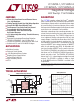


LTC4252-1/LTC4252-2
LTC4252A-1/LTC4252A-2
4
425212fe
For more information www.linear.com/LTC4252-1
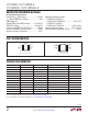
SYMBOL PARAMETER CONDITIONS
LTC4252-1/-2 LTC4252A-1/-2
UNITSMIN TYP MAX MIN TYP MAX
I
TMR
TIMER Pin Current Timer On (Initial Cycle/Latchoff/
Shutdown Cooling, Sourcing),
V
TMR
= 2V
5.8 5.8 µA
Timer Off (Initial Cycle, Sinking),
V
TMR
= 2V
28 28 mA
Timer On (Circuit Breaker, Sourcing,
I
DRN
= 0µA), V
TMR
= 2V
230 230 µA
Timer On (Circuit Breaker, Sourcing,
I
DRN
= 50µA), V
TMR
= 2V
630 630 µA
Timer Off (Circuit Breaker/
Shutdown Cooling, Sinking),
V
TMR
= 2V
5.8 5.8 µA
∆I
TMRACC
/
∆I
DRN
[(I
TMR
at I
DRN
= 50µA) – (I
TMR
at I
DRN
=
0µA)]/∆I
DRN
Timer On (Circuit Breaker with
I
DRN
= 50µA)
8 8 µA/µA
V
DRNL
DRAIN Pin Voltage Low Threshold For PWRGD Status (MS Only) 2.385 2.385 V
I
DRNL
DRAIN Leakage Current V
DRAIN
= 5V (4V for LTC4252A) ±0.1 ±1 ±0.1 ±1 µA
V
DRNCL
DRAIN Pin Clamp Voltage I
DRN
= 50µA 7 6 V
V
PGL
PWRGD Output Low Voltage I
PG
= 1.6mA (MS Only)
I
PG
= 5mA (MS Only)
●
●
0.2 0.4
1.1
0.2 0.4
1.1
V
V
I
PGH
PWRGD Pull-Up Current V
PWRGD
= 0V (Sourcing) (MS Only)
●
40 58 80 40 58 80 µA
t
SS
SS Default Ramp Period SS Pin Floating, V
SS
Ramps from
0.2V to 2V
180 µs
SS Pin Floating, V
SS
Ramps from
0.1V to 0.9V
230 µs
t
PLLUG
UV Low to Gate Low 0.4 0.4 µs
t
PHLOG
OV High to Gate Low 0.4 0.4 µs
elecTrical characTerisTics
The l denotes the specifications which apply over the full operating
temperature range, otherwise specifications are at T
A
= 25°C. (Note 2)
Note 1: Stresses beyond those listed under Absolute Maximum Ratings
may cause permanent damage to the device. Exposure to any Absolute
Maximum Rating condition for extended periods may affect device
reliability and lifetime.
Note 2: All currents into device pins are positive; all currents out of device
pins are negative. All voltages are referenced to V
EE
unless otherwise
specified.