
Datasheet

LTC4252B-1/LTC4252B-2
LTC4252C-1/LTC4252C-2
19
4252b12f
APPLICATIONS INFORMATION
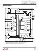
A low impedance short on one card may influence the
behavior of others sharing the same backplane. The initial
glitch and backplane sag as seen in Figure 6 Trace 1, can
rob charge from output capacitors on adjacent cards.
When the faulty card shuts down, current flows in to
refresh the capacitors. If LTC4252s are used by the other
cards, they respond by limiting the inrush
current to a
value of 100mV/R
S
. If C
T
is sized correctly, the capacitors
will recharge long before C
T
times out.
POWER GOOD, PWRGD
PWRGD latches low if GATE charges up to within 2.8V of
V
IN
and DRAIN pulls below V
DRNL
during start-up. PWRGD
is reset in UVLO, in a UV condition or if C
T
charges up to
4V. An overvoltage condition has
no effect on PWRGD
status. A 58µA current pulls this pin high during reset.
Due to voltage transients between the power module and
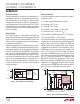
PWRGD, optoisolation is recommended. This pin provides
sufficient drive for an opto-coupler. Figure 19 shows an
alternative NPN configuration with a limiting base resistor
for the PWRGD interface. The module enable input should
have protection from the negative input current.
MOSFET SELECTION
The external MOSFET
switch must have adequate safe
operating area (SOA) to handle short-circuit conditions
until TIMER times out. These considerations take prece-
dence over DC current ratings. A MOSFET with adequate
SOA for a given application can always handle the required
current, but the opposite may not be true. Consult the
manufacturer’s MOSFET data sheet for safe operating
area and effective transient thermal impedance curves.
MOSFET selection
is a 3-step process by assuming the
absence of a soft-start capacitor. First, R
S
is calculated
and then the time required to charge the load capacitance
is determined. This timing, along with the maximum
short-circuit current and maximum input voltage defines
an operating point that is checked against the MOSFET’s
SOA curve.
To begin a design, first specify the required load current
and
Ioad capacitance, I
L
and C
L
. The circuit breaker cur-
rent trip point (V
CB
/R
S
) should be set to accommodate
the maximum load current. Note that maximum input
current to a DC/DC converter is expected at V
SUPPLY(MIN)
.
R
S
is given by:
R
S
=
V
CB(MIN)
I
L(MAX)
(8)
where V
CB(MIN)
= 40mV (45mV for LTC4252C) represents
the guaranteed minimum circuit breaker threshold.
During the initial charging process, the LTC4252B may
operate the MOSFET in current limit, forcing (V
ACL
) between
80mV to 120mV (V
ACL
is 54mV to 66mV for LTC4252C)
across R
S
. The minimum inrush current is given by:
I
INRUSH(MIN)
=
80mV
R
S
(9)
Maximum short-circuit current limit is calculated using
the maximum V
ACL
. This gives
I
SHORTCIRCUIT(MAX)
=
120mV
R
S
(10)
The TIMER capacitor C
T
must be selected based on the
slowest expected charging rate; otherwise TIMER might
time out before the load capacitor is fully charged. A value
for C
T
is calculated based on the maximum time it takes
the load capacitor to charge. That time is given by:
t
CL(CHARGE)
=
C• V
I
=
C
L
• V
SUPPLY(MAX)
I
INRUSH(MIN)
(11)
The maximum current flowing in the DRAIN pin is given by:
I
DRN(MAX)
=
V
SUPPLY(MAX)
–V
DRNCL
R
D
(12)