
Datasheet


LTC4252B-1/LTC4252B-2
LTC4252C-1/LTC4252C-2
30
4252b12f
APPLICATIONS INFORMATION
4252B12 F19
–48RTN
UV
OV
V
EE
V
IN
SENSESS
TIMER GATE
PWRGD
DRAIN
LTC4252C-1
R1
392k
1%
R2
30.1k
1%
C
T
0.68µF
C
SS
68nF
C
C
10nF
–48V
R
S
0.02Ω
Q1
IRF530S
V
OUT
R
C
10Ω
R5
100k
R4
38.3k
D1
BZV85C43
R
IN
3× 1.8k
1/4W EACH
1
9
8
10
3
2
7
6
4
5
C1
10nF
C
IN
1µF
C
L
100µF
–48RTN
(SHORT PIN)
+
R
D
1M
R6 27Ω
LOAD
EN
*
*FMMT493
**DIODES, INC
†
RECOMMENDED FOR HARSH ENVIRONMENTS
D
IN
†
DDZ13B
**
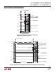
Figure 19. Power Limit Circuit Breaking Application
Circuit Breaker with Foldback Current Limit
Figure 20 shows the LTC4252C in a foldback current
limit application. When V
OUT
is shorted to the –48V RTN
supply, current flows through resistors R4 and R5. This
results in a voltage drop across R5 and a corresponding
reduction in voltage drop across the sense resistor, R
S
,
as the ACL amplifier servos the sense voltage between
the SENSE and V
EE
pins to about 60mV. The short-circuit
current through R
S
reduces as the V
OUT
voltage increases
during an output short-circuit condition. Without foldback
current limiting resistor R5, the current is limited to 3A
during analog current limit. With R5, the short-circuit
current is limited to 0.5A when V
OUT
is shorted to 71V.
Inrush Control Without a Sense
Resistor
During Power-Up
Figure 21 shows the LTC4252C in an application where the
inrush current is controlled without a sense resistor during
power-up. This setup is suitable only for applications that
don’t require short-circuit protection from the LTC4252C.
Resistor R4 and capacitor C2 act as a feedback network
to accurately control the inrush current. The C2 capacitor
can be calculated with the
following equation:
C2=
I
GATE
•C
L
I
INRUSH
(19)
where I
GATE
= 58µA and C
L
is the total load capacitance.
Capacitor C3 and resistor R4 prevent Q1 from momen-
tarily turning on when the power pins first make contact.
Without C3 and R4, capacitor C2 pulls the gate of Q1 up
to a voltage roughly equal to V
EE
• C2/C
GS(Q1)
before the
LTC4252C powers up. By placing capacitor C3 in parallel
with the gate capacitance of Q1 and isolating them from
C2 using resistor R4, the problem is solved. The value of
C3 is given by:
C3=
V
SUPPLY(MAX)
V
GS(TH),Q1
• C2+C
GD(Q1)
( )
(20)
C3 ≈ 35 • C2 for V
SUPPLY(MAX)
= 71V
where V
GS(TH),Q1
is the MOSFET’s minimum gate threshold
and V
SUPPLY(MAX)
is the maximum operating input voltage.
Diode-ORing
Figure 22 shows the LTC4252B used as diode-oring with
Hot Swap capability in a dual –48V power supply applica-
tion. The conventional diode-OR method uses two high
power diodes and heat sinks to contain
the large heat
dissipation of the diodes. With the LTC4252B controlling
the external FETs Q2 and Q3 in a diode-OR manner, the
small turn-on voltage across the fully enhanced Q2 and
Q3 reduces the power dissipation significantly.