
Datasheet


LTC4252B-1/LTC4252B-2
LTC4252C-1/LTC4252C-2
31
4252b12f
APPLICATIONS INFORMATION
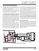
4252B12 F20
UV
OV
V
EE
V
IN
SENSESS
TIMER GATE
PWRGD
DRAIN
LTC4252C-1
R1
392k
1%
R2
30.1k
1%
C
T
0.68µF
C
SS
68nF
C
C
10nF
–48V
R
S
0.02Ω
R4
38.3k
Q1
IRF530S
V
OUT
R
C
10Ω
R3
5.1k
R
IN
3× 1.8k
1/4W EACH
1
9
8
10
3
2
7
6
4
5
C1
10nF
C
IN
1µF
C
L
100µF
–48RTN
(SHORT PIN)
–48RTN
R
D
1M
R5 27Ω
R
G
10Ω
LOAD
EN
*
*MOC207
+
**DIODES, INC
†
RECOMMENDED FOR HARSH ENVIRONMENTS
D
IN
†
DDZ13B
**
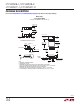
4252B12 F21
UV
OV
V
EE
V
IN
SENSESS
TIMER GATE
PWRGD
DRAIN
LTC4252C-1
R1
392k
1%
R2
30.1k
1%
C
T
0.68µF
C
SS
68nF
C3
330nF
25V
C2
10nF
100V
–48V
R4
1k
1%
Q1
IRF530S
V
OUT
R3
5.1k
R
IN
3× 1.8k
1/4W EACH
1
9
8
10
3
2
7
6
4
5
C1
10nF
C
IN
1µF
C
L
100µF
–48RTN
(SHORT PIN)
–48RTN
R
D
1M
R
G
10Ω
LOAD
EN
*
*MOC207
**DIODES, INC
†
RECOMMENDED FOR HARSH ENVIRONMENTS
D
IN
†
DDZ13B
**
+
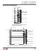
Figure 20. Circuit Breaker with Foldback Current Limit Application
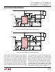
Figure 21. Inrush Control Without a Sense Resistor Application
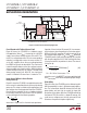
At power-up, Q5 and Q8 are held off low by the SS pin of
the LTC4252B; resistors R5 and R8 pull the SENSE pin
closed to V
EE
. V
EE
is connected to the power supply with
lower voltage through the body diodes Q2 or Q3 until Q2
or Q3 is turned on. This allows the LTC4252B to perform
a start-up cycle and ramp up the SS and GATE voltage.
As the SS voltage ramps up to 2.2V, it turns on Q5 and Q8
and pulls TIMER low through Q6 and Q9. The sense voltage
rises as current flows into R5 and R8 through resistors
R3 and R6. The ACL amplifier of the LTC4252B servos
the sense voltage to about 100mV as the GATE voltage
regulates Q2 and Q3. Current flows into R4, Q4 and R7,
Q7 as Q2 and Q3 turn on. The respective node voltages at
the R3 and R4 connection and the R6 and R7 connection
are always kept equal to their respective sense voltages
by the Q4 and Q2 V
DS
drop and the Q7 and Q3 V
DS
drop
assuming the Q5 and Q8 V
DS
drop is negligible.