
Datasheet

LTC4266
25
4266fe
For more information www.linear.com/LTC4266
Four commonly available 1Ω resistors (0402 or larger
package size) can be used in parallel in place of a single
0.25Ω resistor. In order to meet the I
CUT
and I
LIM
accuracy
required by the IEEE specification, the sense resistors
should have ±1% tolerance or better, and no more than
±200ppm/°C temperature coefficient.
Output Cap
Each port requires a 0.22μF cap across its outputs to keep
the LTC4266 stable while in current limit during startup
or overload. Common ceramic capacitors often have sig-
nificant voltage coefficients; this means the capacitance
is reduced as the applied voltage increases. To minimize
this problem, X7R ceramic capacitors rated for at least
100V are recommended.
ESD/Cable Discharge Protection
Ethernet ports can be subject to significant ESD events
when long data cables, each potentially charged to thou-
sands of volts, are plugged into the low impedance of the
RJ45 jack. To protect against damage, each port requires a
pair of clamp diodes; one to AGND and one to V
EE
(Figure
10). An additional surge suppressor is required for each
LTC4266 chip from V
EE
to AGND. The diodes at the ports
steer harmful surges into the supply rails, where they are
absorbed by the surge suppressor and the V
EE
bypass
capacitance. The surge suppressor has the additional
benefit of protecting the LTC4266 from transients on the
V
EE
supply.
S1B diodes work well as port clamp diodes, and an
SMAJ58A or equivalent is recommended for the V
EE
surge
suppressor.
LAYOUT GUIDELINES
Standard power layout guidelines apply to the LTC4266:
place the decoupling caps for the V
DD
and V
EE
supplies
near their respective supply pins, use ground planes, and
use wide traces wherever there are significant currents.
The main layout challenge involves the arrangement of
the current sense resistors, and their connections to
the LTC4266. Because the sense resistor values are very
low, layout parasitics can cause significant errors. Care is
required to achieve specified accuracy, particularly with
disconnect currents.
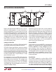
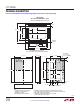
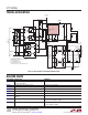
Figure 19 illustrates the problem. In the example on the
left, two ports have load currents I
1
and I
2
that return to
the V
EE
power supply through a mutual resistance R
M
.
R
M
represents the combined resistances of any traces,
planes, and vias in the PCB that I
1
and I
2
share as they
return to the V
EE
supply. The LTC4266 measures the volt-
age difference between its SENSE and V
EE
pins to sense
the voltage drop across R
S1
, but as the example shows,
R
M
introduces errors.
The example on the right shows how errors can be
minimized with a good layout. The circuit is rearranged
so that R
M
no longer affects V
S
, and the V
EE
connection
to the LTC4266 is used as a Kelvin sense trace. V
EE
is not
ApplicAtions inForMAtion
R
M
+
V
S
+
V
S
R
S1
MUTUAL RESISTANCE
R
S2
4266 F19
I
EE
– –
I
1
I
2
I
1
+ I
2
+ I
EE
V
S
= I
1
R
S1
+ I
1
R
M
+ I
2
R
M
LTC4266
GATE
SENSE
SIGNAL
SCALE ERROR
CROSSTALK ERROR
V
EE
R
K
R
M
R
S1
KELVIN SENSE LINE
R
S2
I
EE
I
1
I
2
V
S
= I
1
R
S1
– I
EE
R
K
I
1
+ I
2
+ I
EE
LTC4266
GATE
SENSE
SIGNAL
SMALL OFFSET ERROR
V
EE
Figure 19. Layout Affects Current Readback Accuracy