
Datasheet
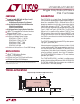

LTC4274A/LTC4274C
6
4274acfc
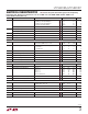
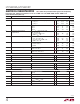
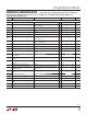
SYMBOL PARAMETER CONDITIONS MIN TYP MAX UNITS
I
2
C Timing
Clock Frequency (Note 7)
l
1 MHz
t
1
Bus Free Time Figure 5 (Notes 7, 9)
l
480 ns
t
2
Start Hold Time Figure 5 (Notes 7, 9)
l
240 ns
t
3
SCL Low Time Figure 5 (Notes 7, 9)
l
480 ns
t
4
SCL High Time Figure 5 (Notes 7, 9)
l
240 ns
t
5
Data Hold Time Figure 5 (Notes 7, 9) Data into Chip
Data Out of Chip
l
l
60
120
ns
ns
t
6
Data Set-Up Time Figure 5 (Notes 7, 9)
l
80 ns
t
7
Start Set-Up Time Figure 5 (Notes 7, 9)
l
240 ns
t
8
Stop Set-Up Time Figure 5 (Notes 7, 9)
l
240 ns
t
r
SCL, SDAIN Rise Time Figure 5 (Notes 7, 9)
l
120 ns
t
f
SCL, SDAIN Fall Time Figure 5 (Notes 7, 9)
l
60 ns
Fault Present to INT Pin Low (Notes 7, 9, 10)
l
150 ns
Stop Condition to INT Pin Low (Notes 7, 9, 10)
l
1.5 µs
ARA to INT Pin High Time (Notes 7, 9)
l
1.5 µs
SCL Fall to ACK Low (Notes 7, 9)
l
120 ns
Note 1: Stresses beyond those listed under Absolute Maximum Ratings
may cause permanent damage to the device. Exposure to any Absolute
Maximum Rating condition for extended periods may affect device
reliability and lifetime.
Note 2: This IC includes overtemperature protection that is intended
to protect the device during momentary overload conditions. Junction
temperature will exceed 140°C when overtemperature protection is active.
Continuous operation above the specified maximum operating junction
temperature may impair device reliability.
Note 3: All currents into device pins are positive; all currents out of device
pins are negative.
Note 4: The LTC4274A/LTC4274C operates with a negative supply voltage
(with respect to ground). To avoid confusion, voltages in this data sheet
are referred to in terms of absolute magnitude.
Note 5: t
DIS
is the same as t
MPDO
defined by IEEE 802.3at.
Note 6: The LTC4274A/LTC4274C digital interface operates with respect to
DGND. All logic levels are measured with respect to DGND.
Note 7: Guaranteed by design, not subject to test.
Note 8: The IEEE 802.3af specification allows a PD to present its
Maintain Power Signature (MPS) on an intermittent basis without being
disconnected. In order to stay powered, the PD must present the MPS for
t
MPS
within any t
MPDO
time window.
Note 9: Values measured at V
ILD(MAX)
and V
IHD(MIN)
.
Note 10: If fault condition occurs during an I
2
C transaction, the INT pin
will not be pulled down until a stop condition is present on the I
2
C bus.
Note 11: Load Characteristic of the LTC4274A/LTC4274C during Mark:
7V < (AGND – V
OUT
) < 10V or I
OUT
< 50µA
Note 12: See the LTC4274A/LTC4274C Software Programming
documentation for information on serial bus usage and device
configuration and status registers.
ELECTRICAL CHARACTERISTICS
The l denotes the specifications which apply over the full operating
temperature range, otherwise specifications are at T
A
= 25°C. AGND – V
EE
= 54V, AGND = DGND, and V
DD
– DGND = 3.3V unless
otherwise noted. (Notes 3, 4)