
Datasheet


LTC4300-1/LTC4300-2
10
430012fb
For more information www.linear.com/LTC4300-1
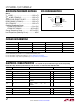
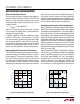
Resistor Pull-Up Value Selection
The system pull-up resistors must be strong enough to
provide a positive slew rate of 1.25V/µs on the SDA and
SCL pins, in order to activate the boost pull-up currents
during rising edges. Choose maximum resistor value R
using the formula:
R ≤ (V
CC(MIN)
– 0.6) (800,000) / C
where R is the pull-up resistor value in ohms, V
CC(MIN)
is the minimum V
CC
voltage and C is the equivalent bus
capacitance in picofarads (pF).
In addition, regardless of the bus capacitance, always
choose R ≤ 16k for V
CC
= 5.5V maximum, R ≤ 24k for
V
CC
=3.6V maximum. The start-up circuitry requires logic
high voltages on SDAOUT and SCLOUT to connect the
backplane to the card, and these pull-up values are needed
to overcome the precharge voltage. See the curves in
Figures 3 and 4 for guidance in resistor pull-up selection.
Minimum SDA and SCL Capacitance Requirements
The LTC4300 I/O connection circuitry requires a minimum
capacitance loading on the SDA and SCL pins in order to
function properly. The value of this capacitance is a func
-
tion of V
CC
and the bus pull-up resistance. Estimate the
bus capacitance on both the
backplane and the card data
and clock busses, and refer to Figures 3 and 4 to choose
appropriate pull-up resistor values. Note from the figures
applicaTions inFormaTion
that 5V systems must have at least 47pF capacitance on
their busses and 3.3V systems must have at least 22pF
capacitance for proper operation of the LTC4300. For ap
-
plications with less capacitance, add a capacitor to ground
to ensure these minimum capacitance conditions.
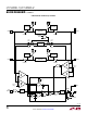
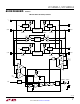
Hot Swapping and Capacitance Buffering Application
Figures 5 through 8 illustrate the usage of the LTC4300 in
applications that take advantage of both its hot swapping
and capacitance buffering features. In all of these applica
-
tions, note that if the I/O cards were plugged directly into
the backplane, all of the backplane and card capacitances
would add directly together, making rise and fall time
requirements difficult to meet. Placing a LTC4300 on the
edge of each card, however, isolates the card capacitance
from the backplane. For a given I/O card, the LTC4300
drives the capacitance of everything on the card and the
backplane must drive only the capacitance of the LTC4300,
which is less than 10pF.
Figure 5 shows the LTC4300-1 in a CompactPCI configura-
tion. Connect V
CC
to the output of one of the CompactPCI
power supply Hot Swap circuits and connect ENABLE
to the short “board ENABLE” pin. V
CC
is monitored by
a filtered UVLO circuit. With the V
CC
voltage powering
up after all other pins have established connection, the
UVLO circuit ensures that the backplane and card data
and clock busses are not connected until the transients
Figure 3. Bus Requirements for 3.3V Systems Figure 4. Bus Requirements for 5V Systems
C
BUS
(pF)
0
R
PULLUP
(kΩ)
430012 F03
30
25
20
15
10
5
0
100 200 300 400
R
MAX
= 24k
RISE TIME > 300ns
RECOMMENDED
PULL-UP
C
BUS
(pF)
0
R
PULLUP
(kΩ)
430012 F04
0
0
5
10
15
20
100
200 300 400
RISE TIME
> 300ns
RECOMMENDED
PULL-UP
R
MAX
= 16k