
Datasheet


LTC4300-1/LTC4300-2
9
430012fb
For more information www.linear.com/LTC4300-1
operaTion
resistors and 100pF equivalent capacitance on both sides
of the part. By comparison with Figure 2, the V
CC
= 3.3V
curve shows that increasing the capacitance from 50pF
to 150pF results in a t
PHL
increase from 55ns to 75ns.
Larger output capacitances translate to longer delays (up to
150ns). Users must quantify the difference in propagation
times for a rising edge vs a falling edge in their systems
and adjust setup and hold times accordingly.
Rise Time Accelerators
Once connection has been established, rise time accelerator
circuits on all four SDA and SCL pins are activated. These
allow the user to choose weaker DC pull-up currents on
the bus, reducing power consumption while still meet
-
ing system
rise time requirements. During positive bus
transitions, the LTC4300 switches in 2mA of current to
quickly slew the SDA and SCL lines once their DC voltages
exceed 0.6V. Using a general rule of 20pF of capacitance
for every device on the bus (10pF for the device and 10pF
for interconnect), choose a pull-up current so that the
bus will rise on its own at a rate of at least 1.25V/µs to
guarantee activation of the accelerators.
For example, assume
an SMBus system with V
CC
= 3V,
a 10k pull-up resistor and equivalent bus capacitance
of 200pF. The
rise time of an SMBus system is calcu-
lated from
(V
IL(MAX)
– 0.15V) to (V
IH(MIN)
+ 0.15V),
or 0.65V to 2.25V. It takes an RC circuit 0.92 time
constants to traverse this voltage for a 3V supply; in this
case, 0.92 • (10k • 200pF) = 1.85µs. Thus, the system
exceeds the maximum allowed rise time of 1µs by 85%.
However, using the rise time accelerators, which are ac-
tivated at a DC threshold of below 0.65V, the worst-case
rise time is: (2.25V – 0.65V) • 200pF/1mA = 320ns, which
meets the 1µs rise time requirement.
READY Digital Output (LTC4300-1)
This pin provides a digital flag which is low when either
ENABLE is low or the start-up sequence described earlier
in this section has not been completed. READY goes HIGH
when ENABLE is high and start-up is complete. The pin
is driven by an open drain pull-down capable of sinking
3mA while holding 0.4V on the pin. Connect a resistor of
10k to V
CC
to provide the pull-up. This feature is available
for the LTC4300-1 only.
ENABLE Low
Current Disable (LTC4300-1)
Grounding
the ENABLE pin disconnects the backplane side
from the card side, disables the rise time accelerators,
drives READY low, disables the bus precharge circuitry
and puts the part in a near-zero current state. When the
pin voltage is driven all the way to V
CC
, the part waits for
data transactions on both the backplane and card sides to
be complete (as described in the Start-Up section) before
reconnecting the two sides. This feature is available for
the LTC4300-1 only.
ACC Boost Current Enable (LTC4300-2)
Users having lightly loaded systems may wish to disable
the rise time accelerators. Driving this pin to ground turns
off the rise time accelerators on all four SDA and SCL
pins. Driving this pin to the V
CC2
voltage enables normal
operation of the rise time accelerators, as described in
the Rise time Accelerators section above. This feature is
available for the LTC4300-2 only.
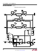
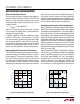
Figure 1. Input–Output Connection t
PLH
Figure 2. Input–Output Connection t
PHL
OUTPUT
SIDE
50pF
430012 F01
INPUT
SIDE
150pF
INPUT
SIDE
150pF
430012 F02
OUTPUT
SIDE
50pF