
Datasheet


LTC4300A-1/LTC4300A-2
14
4300a12fa
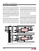
APPLICATIONS INFORMATION
rise- and fall-time specifications for 1nF of capacitance,
thus allowing much more interconnect distance. In this
situation, the differential ground voltage between the two
systems may limit the allowed distance, because a valid
logic low voltage with respect to the ground at one end
of the system may violate the allowed V
OL
specification
with respect to the ground at the other end. In addition,
the connection circuitry offset voltages of the back-to-
back LTC4300A-1s add together, directly contributing
to the same problem.
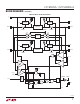
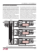
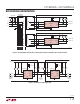
Systems with Disparate Supply Voltages
(LTC4300A-1)
In large 2-wire systems, the V
CC
voltages seen by devices
at various points in the system can differ by a few hun-
dred millivolts or more. This situation is well modelled
by a series resistor in the V
CC
line, as shown in Figure 8.
For proper operation of the LTC4300A-1, make sure that
V
CC(BUS)
≥ V
CC(LTC4300A)
– 0.5V.
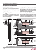
5V to 3.3V Level Translator and Power Supply
Redundancy (LTC4300A-2)
Systems requiring different supply voltages for the back-
plane side and the card side can use the LTC4300A-2, as
shown in Figure 9. The pull-up resistors on the card side
connect from SDAOUT to SCLOUT to V
CC2
, and those on
the backplane side connect from SDAIN and SCLIN to V
CC
.
The LTC4300A-2 functions for voltages ranging from 2.7V
to 5.5V on both V
CC
and V
CC2
. There is no constraint on
the voltage magnitudes of V
CC
and V
CC2
with respect to
each other.
This application also provides power supply redundancy.
If the V
CC2
voltage falls below its UVLO threshold, the
LTC4300A-2 disconnects the backplane from the card,
so that the backplane can continue to function. If the V
CC
voltage falls below its UVLO threshold and the V
CC2
volt-
age remains active, ground the ACC pin to ensure proper
operation.
PACKAGE DESCRIPTION
Please refer to http://www.linear.com/designtools/packaging/ for the most recent package drawings.
MSOP (MS8) 0307 REV F
0.53 ±0.152
(.021 ±.006)
SEATING
PLANE
NOTE:
1. DIMENSIONS IN MILLIMETER/(INCH)
2. DRAWING NOT TO SCALE
3. DIMENSION DOES NOT INCLUDE MOLD FLASH, PROTRUSIONS OR GATE BURRS.
MOLD FLASH, PROTRUSIONS OR GATE BURRS SHALL NOT EXCEED 0.152mm (.006") PER SIDE
4. DIMENSION DOES NOT INCLUDE INTERLEAD FLASH OR PROTRUSIONS.
INTERLEAD FLASH OR PROTRUSIONS SHALL NOT EXCEED 0.152mm (.006") PER SIDE
5. LEAD COPLANARITY (BOTTOM OF LEADS AFTER FORMING) SHALL BE 0.102mm (.004") MAX
0.18
(.007)
0.254
(.010)
1.10
(.043)
MAX
0.22 – 0.38
(.009 – .015)
TYP
0.1016 ±0.0508
(.004 ±.002)
0.86
(.034)
REF
0.65
(.0256)
BSC
0° – 6° TYP
DETAIL “A”
DETAIL “A”
GAUGE PLANE
12
3
4
4.90 ±0.152
(.193 ±.006)
8
7
6
5
3.00 ±0.102
(.118 ±.004)
(NOTE 3)
3.00 ±0.102
(.118 ±.004)
(NOTE 4)
0.52
(.0205)
REF
5.23
(.206)
MIN
3.20 – 3.45
(.126 – .136)
0.889 ±0.127
(.035 ±.005)
RECOMMENDED SOLDER PAD LAYOUT
0.42 ± 0.038
(.0165 ±.0015)
TYP
0.65
(.0256)
BSC
MS8 Package
8-Lead Plastic MSOP
(Reference LTC DWG # 05-08-1660 Rev F)