
Datasheet

LTC4300A-1/LTC4300A-2
4
4300a12fa
–40 25 85
TEMPERATURE (°C)
I
CC
(mA)
4300a12 G01
5.3
5.2
5.1
5.0
4.9
4.8
4.7
4.6
4.5
4.4
4.3
V
CC
= 5.5V
V
CC
= 2.7V
–50 –25 0 25 50 75 100
TEMPERATURE (°C)
I
PULLUPAC
(mA)
4300a12 G03
12
10
8
6
4
2
0
V
CC
= 2.7V
V
CC
= 5V
V
CC
= 3V
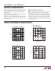
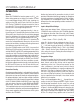
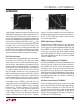
TYPICAL PERFORMANCE CHARACTERISTICS
ELECTRICAL CHARACTERISTICS
I
PULLUPAC
vs Temperature Connection Circuitry V
OUT
– V
IN
I
CC
vs Temperature (LTC4300A-1)
Input – Output t
PHL
vs
Temperature (LTC4300A-1)
Note 1: Stresses beyond those listed under Absolute Maximum Ratings
may cause permanent damage to the device. Exposure to any Absolute
Maximum Rating condition for extended periods may affect device
reliability and lifetime.
Note 2: I
PULLUPAC
varies with temperature and V
CC
voltage, as shown in
the Typical Performance Characteristics section.
Note 3: The connection circuitry always regulates its output to a higher
voltage than its input. The magnitude of this offset voltage as a function of
the pull-up resistor and V
CC
voltage is shown in the Typical Performance
Characteristics section.
Note 4: Guaranteed by design, not subject to test.
Note 5: C
B
= total capacitance of one bus line in pF.
Note 6: These tests measure the difference in high-to-low propagation
delay t
PHL
between the clock and data channels. The delay on each
channel is measured from the 50% point of the falling driven input signal
to the 50% point of the output driven by the LTC4300A-1/LTC4300A-2.
The skew is defined as (t
PHL(SCL)
– t
PHL(SDA)
). Testing is performed in
both directions—from input bus to output bus and vice versa. Tests are
performed with approximately 500pF of distributed equivalent capacitance
on each SDA and SCL pin.
–50 –25 0 25 50 75 100
TEMPERATURE (°C)
t
PHL
(ns)
4300a12 G02
100
80
60
40
20
0
V
CC
= 2.7V
V
CC
= 3.3V
V
CC
= 5.5V
C
IN
= C
OUT
= 100pF
R
PULLUPIN
= R
PULLUPOUT
= 10k
R
PULLUP
(Ω)
0
10,000 20,000 30,000 40,000
V
OUT
– V
IN
(mV)
4300a12 G04
300
250
200
150
100
50
0
V
CC
= 3.3V
V
CC
= 5V
T
A
= 25°C
V
IN
= 0V