
Datasheet

LTC4300A-1/LTC4300A-2
9
4300a12fa
OPERATION
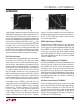
supply voltage, temperature and the pull-up resistors and
equivalent bus capacitances on both sides of the bus. The
Typical Performance Characteristics section shows t
PHL
as a function of temperature and voltage for 10k pull-up
resistors and 100pF equivalent capacitance on both sides
of the part. By comparison with Figure 2, the V
CC
= 3.3V
curve shows that increasing the capacitance from 50pF
to 100pF results in a t
PHL
increase from 55ns to 75ns.
Larger output capacitances translate to longer delays (up
to 150ns). Users must quantify the difference in propaga-
tion times for a rising edge versus a falling edge in their
systems and adjust setup and hold times accordingly.
Rise-Time Accelerators
Once connection has been established, rise-time accelera-
tor circuits on all four SDA and SCL pins are activated.
These allow the user to choose weaker DC pull-up cur-
rents on the bus, reducing power consumption while still
meeting system rise-time requirements. During positive
bus transitions, the LTC4300A switches in 2mA (typical)
of current to quickly slew the SDA and SCL lines once
their DC voltages exceed 0.6V. Using a general rule of
20pF of capacitance for every device on the bus (10pF for
the device and 10pF for interconnect), choose a pull-up
current so that the bus will rise on its own at a rate of at
least 1.25V/μs to guarantee activation of the accelerators.
For example, assume an SMBus system with V
CC
= 3V,
a 10k pull-up resistor and equivalent bus capacitance of
200pF. The rise-time of an SMBus system is calculated
from (V
IL(MAX)
– 0.15V) to (V
IH(MIN)
+ 0.15V), or 0.65V
to 2.25V. It takes an RC circuit 0.92 time constants to
traverse this voltage for a 3V supply; in this case, 0.92
• (10k • 200pF) = 1.84μs. Thus, the system exceeds the
maximum allowed rise-time of 1μs by 84%. However,
using the rise-time accelerators, which are activated at a
DC threshold of below 0.65V, the worst-case rise-time is:
(2.25V – 0.65V) • 200pF/1mA = 320ns, which meets the
1μs rise-time requirement.
READY Digital Output (LTC4300A-1)
This pin provides a digital flag which is low when either
ENABLE is low or the start-up sequence described earlier
in this section has not been completed. READY goes high
when ENABLE is high and start-up is complete. The pin
is driven by an open drain pull-down capable of sinking
3mA while holding 0.4V on the pin. Connect a resistor of
10k to V
CC
to provide the pull-up. This feature is available
for the LTC4300A-1 only.
ENABLE Low Current Disable (LTC4300A-1)
Grounding the ENABLE pin disconnects the backplane side
from the card side, disables the rise-time accelerators,
drives READY low, disables the bus precharge circuitry
and puts the part in a near-zero current state. When the
pin voltage is driven all the way to V
CC
, the part waits for
data transactions on both the backplane and card sides to
be complete (as described in the Start-Up section) before
reconnecting the two sides. This feature is available for
the LTC4300A-1 only.
ACC Boost Current Enable (LTC4300A-2)
Users having lightly loaded systems may wish to disable
the rise-time accelerators. Driving this pin to ground turns
off the rise-time accelerators on all four SDA and SCL
pins. Driving this pin to the V
CC2
voltage enables normal
operation of the rise-time accelerators, as described in
the Rise-Time Accelerators section above. This feature is
available for the LTC4300A-2 only.
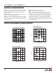
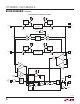
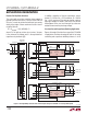
Figure 1. Input–Output Connection t
PLH
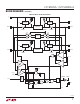
Figure 2. Input–Output Connection t
PHL
OUTPUT
SIDE
50pF
INPUT
SIDE
150pF
4300a12 F01
INPUT
SIDE
150pF
OUTPUT
SIDE
50pF
4300a12 F02