
Datasheet
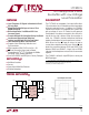

3
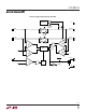
LTC4301L
4301lfa
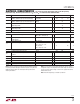
The ● indicates specifications which apply over the full operating
temperature range, otherwise specifications are at T
A
= 25°C. V
CC
= 2.7V to 5.5V, unless otherwise noted.
ELECTRICAL CHARACTERISTICS
Note 1: Stresses beyond those listed under Absolute Maximum Ratings
may cause permanent damage to the device. Exposure to any Absolute
Maximum Rating condition for extended periods may affect device
reliability and lifetime.
Note 2: The connection circuitry always regulates its output to a higher
voltage than its input. The magnitude of this offset voltage as a function of
the pull-up resistor and V
CC
voltage is shown in the Typical Performance
Characteristics section.
Note 3: Determined by design, not tested in production.
SYMBOL PARAMETER CONDITIONS MIN TYP MAX UNITS
V
THR
SDAIN, SCLIN Logic Input Threshold Voltage Rising Edge 0.45 0.6 0.75 V
SDAOUT, SCLOUT Logic Input Threshold Voltage Rising Edge 1.55 1.8 2.0 V
V
HYS
SDAIN, SCLIN Logic Input Threshold Hysteresis (Note 3) 85 mV
SDAOUT, SCLOUT Logic Input Threshold Hysteresis (Note 3) 50 mV
t
PLH
CS Delay On-Off 10 ns
READY Delay Off-On 10 ns
t
PHL
CS Delay Off-On 95 µs
READY Delay On-Off 10 ns
I
OFF
Ready Off Leakage Current ±0.1 µA
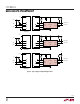
Input-Output Connection
V
OS
Input-Output Offset Voltage 10k to V
CC
on SDA, SCL, V
CC
= 3.3V, ● 0 100 175 mV
SDA or SCL = 0.2V (Note 2)
C
IN
Digital Input Capacitance SDAIN, SDAOUT, (Note 3) 10 pF
SCLIN, SCLOUT
I
LEAK
Input Leakage Current SDA, SCL Pins ±5 µA
V
OL
Output Low Voltage, Input = 0V SDA, SCL Pins, ● 0 0.4 V
I
SINK
= 3mA, V
CC
= 2.7V
SDA, SCL Pins, 0 0.2 V
I
SINK
= 1mA, V
CC
= 2.7V
Timing Characteristics
f
I2C,MAX
I
2
C Maximum Operating Frequency (Note 3) 400 600 kHz
t
BUF
Bus Free Time Between Stop and Start (Note 3) 1.3 µs
Condition
t
HD,STA
Hold Time After (Repeated) Start Condition (Note 3) 100 ns
t
SU,STA
Repeated Start Condition Set-Up Time (Note 3) 0 ns
t
SU,STO
Stop Condition Set-Up Time (Note 3) 0 ns
t
HD,DATI
Data Hold Time Input (Note 3) 0 ns
t
SU,DAT
Data Set-Up Time (Note 3) 100 ns