
Datasheet
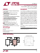

4
LTC4301L
4301lfa
UU
U
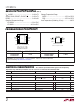
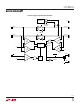
PI FU CTIO S
CS (Pin 1): The connection sense pin is a 1.4V threshold
digital input pin. For normal operation CS is grounded.
Driving CS above the 1.4V threshold isolates SDAIN from
SDAOUT and SCLIN from SCLOUT and asserts READY
low.
SCLOUT (Pin 2): Serial Clock Output. Connect this pin to
the SCL bus on the card.
SCLIN (Pin 3): Serial Clock Input. Connect this pin to SCL
on the bus backplane.
GND (Pin 4, 9): Ground. Connect this pin to a ground plane
for best results. Exposed pad (DFN package) is ground.
READY (Pin 5): The READY pin is an open drain N-channel
MOSFET output which pulls down when CS is high or
when the start-up sequence described in the Operation
section has not been completed. READY goes high when
CS is low and a start-up is complete.
SDAIN (Pin 6): Serial Data Input. Connect this pin to the
SDA bus on the backplane.
SDAOUT (Pin 7): Serial Data Output. Connect this pin to
the SDA bus on the card.
V
CC
(Pin 8): Main Input Supply. Place a bypass capacitor
of at least 0.01µF close to V
CC
for best results.
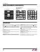
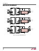
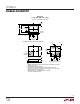
TYPICAL PERFOR A CE CHARACTERISTICS
UW
I
CC
vs Temperature
Input – Output High to Low
Propagation Delay vs
Temperature
Connection Circuitry V
OUT
– V
IN
–50 –25 0 25 50 75 100
TEMPERATURE (°C)
TIME (ns)
4301 G02
100
80
60
40
20
0
V
CC
= 2.7V
V
CC
= 3.3V
V
CC
= 5.5V
C
IN
= C
OUT
= 100pF
R
PULLUPIN
= R
PULLUPOUT
= 10k
R
PULLUP
(Ω)
0
10,000 20,000 30,000 40,000
V
OUT
– V
IN
(mV)
4301 G03
300
250
200
150
100
50
0
V
CC
= 3.3V
V
CC
= 5V
T
A
= 25°C
V
IN
= 0V
TEMPERATURE (°C)
–80
I
CC
(mA)
4.9
4.8
4.7
4.6
4.5
4.4
4.3
4.2
4.1
4.0
3.9
–40
0
20 100
4301 G01
–60 –20
40
60
80
V
CC
= 5.5V
V
CC
= 3.3V
V
CC
= 2.7V