
Datasheet

7
LTC4301L
4301lfa
OPERATIO
U
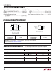
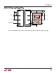
This delay is always positive and is a function of supply
voltage, temperature and the pull-up resistors and equiva-
lent bus capacitances on both sides of the bus. The Typical
Performance Characteristics section shows the high to
low propagation delay as a function of temperature and
voltage for 10k pull-up resistors pulled-up to V
CC
and
100pF equivalent capacitance on both sides of the part.
Larger output capacitances translate to longer delays (up
to 150ns). Users must quantify the difference in propaga-
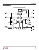
Figure 2. Input-Output Connection
High to Low Propagation Delay
tion times for a rising edge versus a falling edge in their
systems and adjust setup and hold times accordingly.
Ready Digital Output
This pin provides a digital flag which is low when either CS
is high or the start-up sequence described earlier in this
section has not been completed. READY goes high when
CS is low and start-up is complete. The pin is driven by an
open-drain pull-down capable of sinking 3mA while hold-
ing 0.4V on the pin. Connect a resistor of 10k to V
CC
to
provide the pull-up.
Connection Sense
When the CS pin is driven above 1.4V with respect to the
LTC4301L’s ground, the backplane side is disconnected
from the card side and the READY pin is internally pulled
low. When the pin voltage is low, the part waits for data
transactions on both the backplane and card sides to be
complete (as described in the Start-Up section) before
reconnecting the two sides. At this time the internal
pulldown on READY releases.
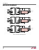
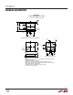
Live Insertion and Capacitance Buffering Application
Figure 3 illustrates applications of the LTC4301L with
different bus pull-up and V
CC
voltages, demonstrating its
ability to recognize and buffer bus data levels that are
above or below its V
CC
supply. All of these applications
take advantage of the LTC4301L’s Hot Swap
TM
controlling,
capacitance buffering and precharge features. If the I/O
cards were plugged directly into the backplane without the
LTC4301L buffer, all of the backplane and card capaci-
tances would add directly together, making rise- and fall-
time requirements difficult to meet. Placing an LTC4301L
on the edge of each card, however, isolates the card
capacitance from the backplane. For a given I/O card, the
LTC4301L drives the capacitance of everything on the card
and the backplane must drive only the capacitance of the
LTC4301L, which is less than 10pF.
APPLICATIO S I FOR ATIO
WUUU
In most applications the LTC4301L will be used with a
staggered connector where V
CC
and GND will be long pins.
SDA and SCL are medium length pins to ensure that the
V
CC
and GND pins make contact first. This will allow the
precharge circuitry to be activated on SDA and SCL before
they make contact. CS is a short pin that is pulled up when
not connected. This is to ensure that the connection
between the backplane and the cards data and clock
busses is not enabled until the transients associated with
live insertion have settled.
Figure 4 shows the LTC4301L in an application where all
of the pins have the same length. In this case, an RC filter
circuit on the I/O card with a product of 10ms provides a
filter to prevent the LTC4301L from becoming activated
until the transients associated with live insertion have
settled. Connect the capacitor between V
CC
and CS, and
the resistor from CS to GND.
Hot Swap is a trademark of Linear Technology Corporation.
4301 F02
INPUT
SIDE
55pF
OUTPUT
SIDE
20pF
0.5V/DIV
20ns/DIV