
Datasheet
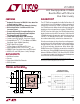

LTC4303
5
4303fb
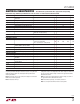
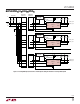
PI FU CTIO S
UUU
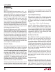
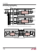
BLOCK DIAGRA
W
ENABLE (Pin 1): Connection Enable. This is a digital
threshold input pin. For normal operation ENABLE is high.
Driving ENABLE below 0.8V isolates SDAIN from SDAOUT,
SCLIN from SCLOUT, asserts READY low and disables
automatic clocking. A rising edge on ENABLE after a fault
has occurred unconditionally forces a connection between
SDAIN, SDAOUT and SCLIN, SCLOUT.
SCLOUT (Pin 2): Serial Clock Output. Connect this pin to
the SCL bus on the card.
SCLIN (Pin 3): Serial Clock Input. Connect this pin to SCL
on the bus backplane.
GND (Pin 4): Device Ground. Connect this pin to a ground
plane for best results.
READY (Pin 5): Connection Status Flag. READY provides
a digital fl ag which indicates the status of the connection
circuitry described in the “Connection Circuitry” section.
Connect a resistor of 10k to V
CC
to provide the pull-up.
SDAIN (Pin 6): Serial Data Input. Connect this pin to the
SDA bus on the backplane.
SDAOUT (Pin 7): Serial Data Output. Connect this pin to
the SDA bus on the card.
V
CC
(Pin 8): Supply Voltage Input. Place a bypass capacitor
of at least 0.01µF close to V
CC
for best results.
Exposed Pad (Pin 9, DFN Only): Exposed pad may be left
open or connected to the ground plane.
LTC4303 2-Wire Bus Buffer with Stuck Bus Protection
CONNECT
PC_CONNECT PC_CONNECT
PC_CONNECT
CONNECT
1
200k
200k
200k
200k
PRECHARGE
LOGIC
30ms
TIMER
95 s
DELAY
1.4V
ENABLE
1.8V
3
SCLIN
6
SDAIN
1.8V
CONNECT
CONNECT
7
SDAOUT
8
V
CC
2
SCLOUT
READY
5
GND
4301 BD
4
SLEW RATE
DETECTOR
3.5mA
SLEW RATE
DETECTOR
3.5mA
SLEW RATE
DETECTOR
3.5mA
SLEW RATE
DETECTOR
3.5mA
UVLO
UVLO
–
+
–
+
–
+
–
+
–
+
AUTOMATIC
CLOCKING