
Datasheet

LTC4303
7
4303fb
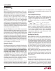
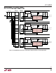
OUTPUT SIDE
50pF
0.5V/DIV
INPUT SIDE
150pF
0.5V/DIV
200ns/DIV
4303 F01
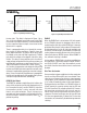
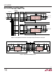
INPUT SIDE
50pF
0.5V/DIV
OUTPUT SIDE
150pF
0.5V/DIV
20ns/DIV
4303 F02
OPERATIO
U
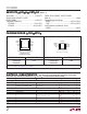
Figure 1. Input-Output Connection t
PLH
the two sides. This effect is displayed in Figure 1 for a
V
CC
= 3.3V and a 10k pull-up resistor on each side (50pF
on one side and 150pF on the other). Since the output side
has less capacitance than the input, it rises faster and the
effective t
PLH
is negative.
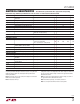
There is a propagation delay, t
PHL
, through the connec-
tion circuitry for falling waveforms. Figure 2 shows the
falling edge waveforms. An external driver pulls down
the voltage on the side with 50pF capacitance; LTC4303
pulls down the voltage on the opposite side with a delay
of 80ns. This delay is always positive and is a function of
supply voltage, temperature and the pull-up resistors and
equivalent bus capacitances on both sides of the bus. The
Typical Performance Characteristics section shows t
PHL
as a function of temperature and voltage for 10k pull-up
resistors and 100pF equivalent capacitance on both sides
of the part. Larger output capacitances translate to longer
delays. Users must quantify the difference in propagation
times for a rising edge versus a falling edge in their systems
and adjust setup and hold times accordingly.
READY Digital Output
The READY pin provides a digital fl ag which indicates the
status of the connection circuitry described previously in
the “Connection Circuitry” section. READY is high when
the connection circuitry is active, and pulls low when
there is not a valid connection. The pin is driven by an
open drain pull-down capable of sinking 3mA while hold-
ing 0.4V on the pin. Connect a resistor of 10k to V
CC
to
provide the pull-up.
ENABLE
When the ENABLE pin is driven below 0.8V with respect
to the LTC4303’s ground, the backplane side is discon-
nected from the card side, and the READY pin is internally
pulled low. When the pin is driven above 2V, the part waits
for data transactions on the IN side to be complete and
for the OUT side to be high (as described in the Start-Up
section) before connecting the two sides. At this time the
internal pull-down on READY releases. When ENABLE is
low, automatic clocking is disabled.
A rising edge on ENABLE after a stuck bus condition has
occurred forces a connection between SDAIN, SDAOUT
and SCLIN, SCLOUT even if bus idle conditions are not
met. At this time the internal 30ms timer is reset but not
disabled.
Rise Time Accelerators
Once connection has been established, rise time accelerator
circuits on all four SDA and SCL pins are activated. These
allow the use of larger pull-up resistors, reducing power
consumption, or bus capacitance beyond that specifi ed
in I
2
C, while still meeting system rise time requirements.
During positive bus transitions, the LTC4303 switches in
3.5mA (typical) of current to quickly slew the SDA and
SCL lines once their DC voltages exceed 0.8V. Choose a
pull-up resistor so that the bus will rise on its own at a
rate of at least 0.8V/µs to guarantee activation of the ac-
celerators. Rise time accelerators turn off when SDA and
SCL lines are approximately 1V below V
CC
.The rise time
accelerators are automatically disabled during automatic
clocking.
Figure 2. Input-Output Connection t
PHL