
Datasheet

LTC4303
8
4303fb
Resistor Pull-Up Selection
The system pull-up resistors must be strong enough
to provide a positive slew rate of 0.8V/µs on the SDA
and SCL pins, in order to activate the rise time accelera-
tors during rising edges. Choose maximum resistor value
R
PULL-UP(MAX)
using the formula:
where V
BUSMIN
is the minimum operating pull-up sup-
ply voltage, and C
BUS
the total capacitance on respec-
tive bus line.
Rk
V V ns V
CpF
PULLUP MAX
BUS MIN
BUS
()
()
[]
–. • [ /]
[]
Ω=
()
0 8 1250
For example, assume V
BUS
= V
CC
= 3.3V, and assuming
±10% supply tolerance, V
BUSMIN
= 2.97V. With C
BUS
=
100pF, R
PULL-UP, MAX
= 27.1k. Therefore a smaller pull-up
resistor than 27.1k must be used, so 10k works fi ne.
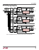
Live Insertion and Capacitance Buffering Application
Figures 3 through 6 illustrate applications of the LTC4303
that take advantage of both its Hot Swap
TM
controlling and
capacitance buffering features. In all of these applications,
note that if the I/O cards were plugged directly into the
backplane without the LTC4303 buffer, all of the backplane
and card capacitances would add directly together, making
rise- and fall-time requirements diffi cult to meet. Placing a
LTC4303 on the edge of each card, however, isolates the
card capacitance from the backplane. For a given I/O card,
the LTC4303 drives the capacitance on the card side and
the backplane must drive only the digital input capacitance
of the LTC4303, which is less than 10pF.
In most applications the LTC4303 will be used with a
staggered connector where V
CC
and GND will be long
pins. SDA and SCL are medium length pins to ensure that
the V
CC
and GND pins make contact fi rst. This will allow
the precharge circuitry to be activated on SDA and SCL
before they make contact. ENABLE is a short pin that is
pulled down when not connected. This is to ensure that
the connection between the backplane and the cards data
and clock busses is not enabled until the transients as-
sociated with live insertion have settled.
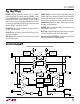
Figure 3 shows the LTC4303 in a CompactPCI
TM
confi gu-
ration. Connect V
CC
and ENABLE to the output of one of
the CompactPCI power supply Hot Swap circuits. Use a
pull-up resistor to ENABLE for a card side enable/disable.
V
CC
is monitored by a fi ltered UVLO circuit. With the V
CC
voltage powering up after all the other pins have established
connection, the UVLO circuit ensures that the backplane
and the card data and clock busses are not connected until
the transients associated with live insertion have settled.
Owing to their small capacitance, the SDAIN and SCLIN
pins cause minimal disturbance on the backplane busses
when they make contact with the connector.
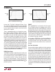
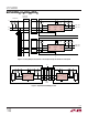
Figure 4 shows the LTC4303 in a PCI application where all
of the pins have the same length. In this case, a RC fi lter
circuit on the I/O card with a product of 10ms provides
a fi lter to prevent the LTC4303 from becoming activated
until the transients associated with live insertion have
settled. Connect the capacitor between ENABLE and GND,
and the resistor from V
CC
to ENABLE.
Hot Swap is a trademark of Linear Technology Corporation.
APPLICATIO S I FOR ATIO
WUU
U