
Datasheet


LTC4304
5
4304fa
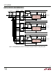
ENABLE (Pin 1): Connection Enable. This is a digital
threshold input pin. For normal operation ENABLE is high.
Driving ENABLE below 0.8V isolates SDAIN from SDAOUT,
SCLIN from SCLOUT, asserts READY low and disables
automatic clocking. A rising edge on ENABLE after a fault
has occurred unconditionally forces a connection between
SDAIN, SDAOUT and SCLIN, SCLOUT.
SCLOUT (Pin 2): Serial Clock Output. Connect this pin to
the SCL bus on the card.
SCLIN (Pin 3): Serial Clock Input. Connect this pin to SCL
on the bus backplane.
ACC (Pin 4): Rise-Time Accelerator Control. Connect ACC
to V
CC
to disable all four accelerators. Connect ACC to
GND to enable all four accelerators. Float ACC to enable
the SDAOUT and SCLOUT accelerators only. For applica-
tions when V
CC
is greater than the bus pull-up voltage,
connect ACC to V
CC
.
GND (Pin 5): Device Ground. Connect this pin to a ground
plane for best results.
READY (Pin 6): Connection Status Flag. READY provides
a digital fl ag which indicates the status of the connection
circuitry described in the “Connection Circuitry” section.
Connect a resistor of 10k to V
CC
to provide the pull-up.
FAULT (Pin 7): Bus Stuck Low Fault. FAULT is an open
drain N-channel MOSFET which pulls low to signal a bus
stuck low condition. In normal operation, FAULT is high.
Connect a 10k resistor from this pin to V
CC
to provide
the pull-up.
SDAIN (Pin 8): Serial Data Input. Connect this pin to the
SDA bus on the backplane.
SDAOUT (Pin 9): Serial Data Output. Connect this pin to
the SDA bus on the card.
V
CC
(Pin 10): Supply Voltage Input. Place a bypass capaci-
tor of at least 0.01µF close to V
CC
for best results.
Exposed Pad (Pin 11, DFN Only): Exposed pad may be
left open or connected to the ground plane.
PI FU CTIO S
UUU