
Datasheet


LTC4304
9
4304fa
A rising edge on ENABLE after a stuck bus condition has
occurred forces a connection between SDAIN, SDAOUT
and SCLIN, SCLOUT even if bus idle conditions are not
met. At this time the internal 30ms timer is reset but not
disabled.
Rise Time Accelerators
Once connection has been established, rise time accel-
erator circuits on all four SDA and SCL pins are activated
(assuming accelerators are enabled, see ACC pin descrip-
tion). These allow the use of a large pull-up resistor to
reduce power consumption, or bus capacitance beyond
that specifi ed in I
2
C, while still meeting system rise time
requirements. During positive bus transitions, the LTC4304
switches in 3.5mA (typical) of current to quickly slew the
SDA and SCL lines once their DC voltages exceed 0.8V.
Choose a pull-up resistor so that the bus will rise on its
own at a rate of at least 0.8V/µs to guarantee activation
of the accelerators. Rise time accelerators turn off when
SDA and SCL lines are approximately 1V below V
CC
.
Rise time accelerators are automatically disabled during
automatic clocking.
Resistor Pull-Up Selection
The system pull-up resistors must be strong enough
to provide a positive slew rate of 0.8V/µs on the SDA
and SCL pins, in order to activate the rise time accelera-
tors during rising edges. Choose maximum resistor value
R
PULL-UP(MAX)
using the formula:
Rk
V V ns V
CpF
PULLUP MAX
BUS MIN
BUS
()
()
[]
–. • [ /]
[]
Ω=
()
0 8 1250
where V
BUSMIN
is the minimum operating pull-up sup-
ply voltage, and C
BUS
the total capacitance on respec-
tive bus line.
For example, assume V
BUS
= V
CC
= 3.3V, and assuming
±10% supply tolerance, V
BUSMIN
= 2.97V. With C
BUS
=
100pF, R
PULL-UP, MAX
= 27.1k. Therefore a smaller pull-up
resistor than 27.1k must be used, so 10k works fi ne.
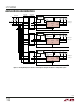
Live Insertion and Capacitance Buffering Application
Figures 3 through 6 illustrate applications of the LTC4304
that take advantage of both its Hot Swap
TM
controlling and
capacitance buffering features. In all of these applications,
note that if the I/O cards were plugged directly into the
backplane without the LTC4304 buffer, all of the backplane
and card capacitances would add directly together, making
rise- and fall-time requirements diffi cult to meet. Placing a
LTC4304 on the edge of each card, however, isolates the
card capacitance from the backplane. For a given I/O card,
the LTC4304 drives the capacitance on the card side and
the backplane must drive only the digital input capacitance
of the LTC4304, which is less than 10pF.
In most applications the LTC4304 will be used with a
staggered connector where V
CC
and GND will be long
pins. SDA and SCL are medium length pins to ensure that
the V
CC
and GND pins make contact fi rst. This will allow
the precharge circuitry to be activated on SDA and SCL
before they make contact. ENABLE is a short pin that is
pulled down when not connected. This is to ensure that the
connection between the backplane and the cards data and
clock busses is not enabled until the transients associated
with live insertion have settled.
Figure 3 shows the LTC4304 in a CompactPCI
TM
confi gura-
tion. Connect V
CC
and ENABLE to the output of one of the
CompactPCI power supply Hot Swap circuits. Use a pull-up
resistor to ENABLE for a card side enable/disable. V
CC
is
monitored by a fi ltered UVLO circuit. With the V
CC
voltage
powering up after all the other pins have established con-
nection, the UVLO circuit ensures that the backplane and
the card data and clock busses are not connected until
the transients associated with live insertion have settled.
Owing to their small capacitance, the SDAIN and SCLIN
pins cause minimal disturbance on the backplane busses
when they make contact with the connector.
Hot Swap is a trademark of Linear Technology Corporation.
OPERATION
APPLICATIONS INFORMATION