
Datasheet

LTC4305
11
4305f
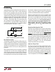
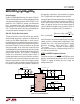
separated by the series combination of their switches’ on
resistances. While neither, either or both downstream
buses may be connected at the same time, logic high
levels are corrupted if both downstream buses are active
and both the V
CC
voltage and one downstream bus pull-up
voltage are larger than the pull-up supply voltage of the
other downstream bus. An example of this issue is shown
in Figure 1. During logic highs, DC current flows from
V
BUS1
through the series combination of R1, N1, N2 and
R2 and into V
BUS2
, causing the SDA1 voltage to drop and
current to be sourced into V
BUS2
. To avoid this problem,
do not activate bus 1 when bus 2 is active.
first, the pin’s voltage is rising at a minimum slew rate of
0.8V/µs; second, the voltages on both the upstream bus
and the connected downstream buses exceed 0.8V.
Note that a downstream bus must be connected to the
upstream bus in order for its rise time accelerator current
to be active. See the Applications Section for choosing a
bus pull-up resistor value to ensure that the rise time
accelerator switches turn on. Do not activate boost cur-
rents on a bus whose pull-up supply voltage V
BUS
< V
CC
.
Doing so would cause the boost currents to source
current from V
CC
into the V
BUS
supply during rising
edges.
Downstream Bus Connection Fault
By default, the LTC4305 will only connect to downstream
buses whose SDA and SCL pins are both high (above 1V)
at the moment that it receives the connection command.
In this case, the LTC4305 sets the Failed Connection
Attempt bit of register 0 low and pulls the ALERT low when
the master tries to connect to a low downstream bus. Note
that users can write a high to the Connection Requirement
bit of register 2 to program the LTC4305 to connect to
downstream buses regardless of their logic state at the
moment of connection. In this case, the Downstream
Channel Connection Fault never occurs.
Stuck Low Timeout Fault
The Stuck Low Timeout Circuitry monitors the two com-
mon internal nodes of the downstream SDA and SCL
switches and runs a timer whenever either of the internal
node voltages is below 0.52V. The timer is reset whenever
both internal node voltages are above 0.6V. If the timer
ever reaches the time programmed by Timeout Mode Bits
1 and 0 of register 2, the LTC4305 pulls ALERT low and
OPERATIO
U
Rise Time Accelerators
The Upstream Accelerators Enable and Downstream Ac-
celerators Enable bits of register 1 activate the upstream
and downstream rise time accelerators, respectively. When
activated, the accelerators turn on in a controlled manner
and source current into the pins during positive bus
transitions.
When no downstream buses are connected, an upstream
accelerator turns on when its pin voltage exceeds 0.8V
and is rising at a minimum slew rate of 0.8V/µs. When one
or more downstream buses are connected, the accelera-
tor on a given pin turns on when these conditions are met:
Figure 1. Example of Unacceptable Level Shifting
SDA2
4305 F01
SDA1
R1
10k
R2
10k
N1
N2
V
CC
= V
BUS1
= 5V
V
BUS2
= 2.5V