
Datasheet

LTC4305
13
4305f
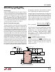
Figure 4. Protocols Accepted by LTC4305
4305 F04
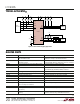
S
ACK
0001 100 Rd DEVICE ADDRESS
1
1
71 8
1
P
1
ACK
START
ACK
10 a4 - a0 WR XXXXXX r1 r0
1
1
71 8
S
00
ACK
1
S
0
REGISTERSLAVE
ADDRESS
START
ACK
10 a4 - a0 RD d7 - d0
1
1
71 8
S
10
S
0
DATA
BYTE
1
M
1
STOP
1
SLAVE
ADDRESS
ACK
M
1
START
ACK
10 a4 - a0 WR XXXXXX r1 r0
1
1
71 8
S
00
ACK
1
S
0
REGISTERSLAVE
ADDRESS
d7 - d0
8
DATA
BYTE
1
S
0
STOP
1
ACK
WRITE BYTE PROTOCOL
READ BYTE PROTOCOL
ALERT RESPONSE ADDRESS PROTOCOL
1
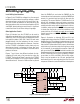
regardless of their individual address settings. The mass
write can be masked by setting the mass write enable bit
of register 2 to zero. Address (0001 100) is the SMBus
Alert Response Address. Figure 3 shows data transfer
over a 2-wire bus.
Supported Commands
Users must write to the LTC4305 using the SMBus Write
Byte protocol and read from it using the Read Byte
protocol. During fault resolution, the LTC4305 also
supports the Alert Response Address protocol. The
formats for these protocols are shown in Figure 4. Users
must follow the Write Byte protocol exactly to write to the
LTC4305; if a Repeated Start Bit is issued before a Stop
Bit, the LTC4305 ignores the attempted write, and its
control bits remain in their preexisting state. When users
follow the WriteByte protocol exactly, the new data con-
tained in the Data Byte is written into the register selected
by r1 and r0 on the Stop Bit.
OPERATIO
U
Glitch Filters
The LTC4305 provides glitch filters on the SDAIN and
SCLIN pins as required by the I
2
C Fast Mode (400kHz)
Specification. The filters prevent signals of up to 50ns
(minimum) time duration and rail-to-rail voltage magni-
tude from passing into the two-wire bus digital interface
circuitry.
Fall Time Control
Per the I
2
C Fast Mode (400kHz) Specification, the
two-wire bus digital interface circuitry provides fall time
control when forcing logic lows onto the SDAIN bus. The
fall time always meets the limits:
(20 + 0.1 • C
B
) < t
f
< 300ns
where t
f
is the fall time in ns and C
B
is the equivalent bus
capacitance in pF. Whenever the upstream-downstream
buffer circuitry is active, its output signal will meet the fall
time requirements, provided that its input signal meets the
fall time requirements.
Figure 3. Data Transfer Over I
2
C/SMBus
SCL
SDA
START
CONDITION
STOP
CONDITION
ADDRESS R/W ACK DATA ACK DATA ACK
1 - 7 8 9
4305 F03
a6 - a0 d7 - d0 d7 - d0
1 - 7 8 9 1 - 7 8 9
P
S