
Datasheet

LTC4305
4305f
4
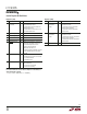
The ● denotes specifications which apply over the full specified temperature
range, otherwise specifications are at T
A
= 25°C. V
CC
= 3.3V unless otherwise noted.
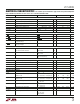
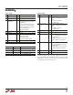
ELECTRICAL CHARACTERISTICS
Note 1: Absolute Maximum Ratings are those values beyond which the life
of a device may be impaired.
Note 2: Guaranteed by design and not subject to test, unless stated
otherwise in the Conditions.
Note 3: The boosted pull-up currents are regulated to prevent excessively
fast edges for light loads. See the Typical Performance Characteristics for
rise time as a function of V
CC
and parasitic bus capacitance C
BUS
and for
I
BOOST
as a function of V
CC
and temperature.
Note 4: When a logic low voltage V
LOW
is forced on one side of the
upstream-downstream buffers, the voltage on the other side is regulated
to a voltage V
LOW2
= V
LOW
+ V
OS
is a positive offset voltage. V
OS,DOWN-BUF
is the offset voltage when the LTC4305 is driving the upstream pin (e.g.,
SDAIN) and V
OS,DOWN-BUF
is the offset voltage when the LTC4305 is
driving the downstream pin (e.g., SDA1). See the Typical Performance
Characteristics for V
OS,UP-BUF
and V
OS,DOWN-BUF
as a function of V
CC
and
bus pull-up current.
Note 5: When floating, the ADR0–ADR2 pins can tolerate pin leakage
currents up to I
ADR,FLOAT
and still convert the address correctly.
SYMBOL PARAMETER CONDITIONS MIN TYP MAX UNITS
I
2
C Interface
V
ADR(H)
ADR0–2 Input High Voltage ● 0.75 • V
CC
0.9 • V
CC
V
V
ADR(L)
ADR0–2 Input Low Voltage ● 0.1 • V
CC
0.25 • V
CC
V
I
ADR(IN, L)
ADR0–2 Logic Low Input Current ADR0–2 = 0V, V
CC
= 5.5V ● –30 –60 –80 µA
I
ADR(IN, H)
ADR0–2 Logic High Input Current ADR0–2 = V
CC
= 5.5V ● 30 60 80 µA
I
ADR,FLOAT
ADR0–2 Allowed Input Current V
CC
= 2.7V, 5.5V (Note 5) ● ±5 ±13 µA
V
SDAIN,SCLIN(TH)
SDAIN, SCLIN Input Falling Threshold Voltages V
CC
= 5.5V ● 1.4 1.6 1.8 V
V
SDAIN,SCLIN(HY)
SDAIN, SCLIN Hysteresis 30 mV
I
SDAIN,SCLIN(OH)
SDAIN, SCLIN Input Current SCL, SDA = V
CC
● ±
5 µA
C
IN
SDA, SCL Input Capacitance (Note 2) 6 10 pF
V
SDAIN(OL)
SDAIN Output Low Voltage I
SDA
= 4mA, V
CC
= 2.7V ● 0.2 0.4 V
I
2
C Interface Timing
f
SCL
Maximum SCL Clock Frequency (Note 2) 400 kHz
t
BUF
Bus Free Time Between Stop/Start Condition (Note 2) 0.75 1.3 µs
t
HD, STA
Hold Time After (Repeated) Start Condition (Note 2) 45 100 ns
t
SU, STA
Repeated Start Condition Set-Up Time (Note 2) –30 0 ns
t
SU, STO
Stop Condition Set-Up Time (Note 2) –30 0 ns
t
HD, DATI
Data Hold Time Input (Note 2) –25 0 ns
t
HD, DATO
Data Hold Time Output (Note 2) 300 600 900 ns
t
SU, DAT
Data Set-Up Time (Note 2) 50 100 ns
t
f
SCL, SDA Fall Times (Note 2) 20 + 0.1 • 300 ns
C
BUS
t
SP
Pulse Width of Spikes Suppressed by the (Note 2) 50 150 250 ns
Input Filter