
Datasheet

LTC4306
11
4306f
Rise Time Accelerators
The Upstream Accelerators Enable and Downstream Ac-
celerators Enable bits of register 1 activate the upstream
and downstream rise time accelerators, respectively.
When activated, the accelerators turn on in a controlled
manner and source current into the pins during positive
bus transitions.
When no downstream buses are connected, an upstream
accelerator turns on when its pin voltage exceeds 0.8V
and is rising at a minimum slew rate of 0.8V/µs. When one
or more downstream buses are connected, the accelera-
tor on a given pin turns on when these conditions are met:
first, the pin’s voltage is rising at a minimum slew rate of
0.8V/µs; second, the voltages on both the upstream bus
and the connected downstream buses exceed 0.8V.
Note that a downstream bus’s switch must be closed in
order for its rise time accelerator current to be active. See
the Applications Section for choosing a bus pull-up resis-
tor value to ensure that the rise time accelerator switches
turn on. Do not activate boost currents on a bus whose
pull-up supply voltage V
BUS
is less than V
CC
. Doing so
would cause the boost currents to source current from
V
CC
into the V
BUS
supply during rising edges.
Downstream Bus Connection Fault
By default, the LTC4306 will only connect to downstream
channels whose SDA and SCL pins are both high (above
1V) at the moment that it receives the connection com-
mand. In this case, the LTC4306 sets the Failed Connec-
tion Attempt bit of register 0 low and pulls the ALERT pin
low when the master tries to connect to a low downstream
channel. Note that users can write a high to the Connection
Requirement bit of register 2 high to program the LTC4306
to connect to downstream channels regardless of their
logic state at the moment of connection. In this case, the
downstream channel connection fault never occurs.
Stuck Low Timeout Fault
The stuck low timeout circuitry monitors the two common
internal nodes of the downstream SDA and SCL switches
and runs a timer whenever either of the internal node
voltages is below 0.52V. The timer is reset whenever both
internal node voltages are above 0.6V. If the timer ever
reaches the time programmed by Timeout Mode Bits 1 and
0 of register 2, the LTC4306 pulls ALERT low and discon-
nects the downstream bus(es) from the upstream bus by
de-biasing the Upstream-Downstream Buffers. Note that
the downstream switches remain in their existing state.
The Timeout Real-Time bit of register 0 indicates the real-
time status of the stuck low situation. The Latched Timeout
Bit of register 0 is a latched bit that is set high when a
timeout occurs.
External Faults on the Downstream Channels
When a slave on downstream bus 1 pulls the ALERT1 pin
below 1V, the LTC4306 passes this information to the
master on the upstream bus by pulling the ALERT pin low.
The same is true for the other three downstream buses.
Each bus has its own dedicated fault bit in Register 0, so
that masters can read Register 0 to determine which buses
have faults.
ALERT Functionality and Fault Resolution
When a fault occurs, the LTC4306 pulls the ALERT pin low,
as described previously. The procedure for resolving
faults depends on the type of fault. If a master on the
upstream bus is communicating with devices on a down-
stream bus via the Upstream-Downstream Buffer cir-
cuitry—channel 1, for example—and a device on this bus
pulls the ALERT1 pin low, the LTC4306 acts transparently,
and the master communicates directly with the device that
caused the fault via the upstream-downstream buffer
circuitry to resolve the fault.
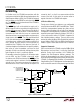
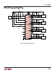
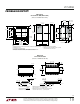
OPERATIO
U
SDA1
N1
N2
4306 F01
SDA2
V
CC
= V
BUS1
= 5V
V
BUS2
= 2.5V
R1
10k
R2
10k
Figure 1. Example of Unacceptable Level Shifting