
Datasheet

LTC4306
4306f
14
OPERATIO
U
is 35Ω, making the GPIO pull-downs capable of driving
LEDs. At V
CC
= 5V, the typical pull-up impedance is 320Ω
and the typical pull-down impedance is 20Ω. In open-
drain output mode, the user provides the logic high by
connecting a pull-up resistor between the GPIO pin and an
external supply voltage. The external supply voltage can
range from 1.5V to 5.5V independent of the V
CC
voltage.
In input mode, the GPIO input threshold voltage is 1V.
The GPIO1 and GPIO2 Logic State bits in register 1
indicate the logic state of the two GPIO pins. The logic-
level threshold voltage for each pin is 1V. The GPIO1 and
GPIO2 Output Driver State bits in register 1 indicate the
logic state that the LTC4306 is attempting to write to the
GPIO pins. This is useful when the GPIOs are being used
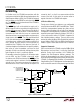
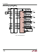
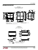
Figure 4. Protocols Accepted by LTC4306
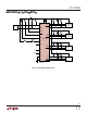
Figure 3. Data Transfer Over I
2
C or SMBus
SCL
SDA
START
CONDITION
STOP
CONDITION
ADDRESS R/W ACK DATA ACK DATA ACK
1-7 8 9
4306 F03
a6-a0 d7-d0 d7-d0
1-7 8 9 1-7 8 9
P
S
4306 F04
S
0001 100 RD DEVICE ADDRESS
1
1
71 8
1
P
1
START
ACK
10 a4-a0 WR XXXXXX r1r0
1
1
71 8
S
00
ACK
1
S
0
ACK
S
0
ACK
M
1
REGISTERSLAVE
ADDRESS
START
ACK
10 a4-a0 RD d7-d0
1
1
71 8
S
10
DATA
BYTE
1
M
1
STOP
1
SLAVE
ADDRESS
ACK
START
ACK
10 a4-a0 WR XXXXXX r1r0
1
1
71 8
S
00
ACK
1
S
0
REGISTERSLAVE
ADDRESS
d7-d0
8
DATA
BYTE
1
S
0
STOP
1
ACK
WRITE BYTE PROTOCOL
READ BYTE PROTOCOL
ALERT RESPONSE ADDRESS PROTOCOL
1
in open-drain output mode and one or more external
devices are connected to the GPIOs. If the LTC4306 is
trying to write a high to a GPIO pin, but the pin’s actual
logic state is low, then the LTC4306 knows that the low is
being forced by an external device.
Glitch Filters
The LTC4306 provides glitch filters on the SDAIN and
SCLIN pins as required by the I
2
C Fast Mode (400kHz)
Specification. The filters prevent signals of up to 50ns
(minimum) time duration and rail-to-rail voltage
magnitude from passing into the two-wire bus digital
interface circuitry.