
Datasheet

LTC4306
15
4306f
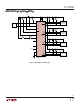
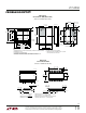
Design Example
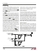
A typical LTC4306 application circuit is shown in Figure 5.
The circuit illustrates the level-shifting, multiplexer/switch
and capacitance buffering features of the LTC4306. In this
application, the LTC4306 V
CC
voltage and downstream
bus 1 are powered from a 3.3V supply voltage; down-
stream bus 4 is powered from 5V, and the upstream bus
is powered from 2.5V. Channels 2 and 3 are omitted for
simplicity. The following sections describe a methodology
for choosing the external components in Figure 5.
SDA, SCL Pull-Up Resistor Selection
The pull-up resistors on the SDA and SCL pins must be
strong enough to provide a minimum of 100µA pull-up
current, per the SMBus Specification. In most systems,
the required minimum strength of the pull-up resistors is
determined by the minimum slew requirement to guaran-
tee that the LTC4306’s rise time accelerators are activated
during rising edges. At the same time, the pull-up value
should be kept low to maximize the logic low noise margin
and minimize the offset voltage of the Upstream-Down-
stream Buffer circuitry. The LTC4306 is designed to func-
tion for a maximum DC pull-up current of 4mA. If multiple
downstream channels are active at the same time, this
means that the sum total of the pull-up currents from these
channels must be less than 4mA. At supply voltages of
2.7V and 5.5V, pull-up resistor values of 10k work well for
capacitive loads up to 215pF and 420pF, respectively. For
larger bus capacitances, refer to equation (1) below. The
LTC4306 works with capacitive loads up to 2nF.
APPLICATIO S I FOR ATIO
WUUU
Figure 5. A Level Shifting Circuit
Fall Time Control
Per the I
2
C Fast Mode (400kHz) Specification, the two-
wire bus digital interface circuitry provides fall time con-
trol when forcing logic lows onto the SDAIN bus. The fall
time always meets the limits:
(20 + 0.1 • C
B
) < t
f
< 300ns
V
CC
C1
0.01µF
V
CC
= V
BUS1
= 3.3V
V
BACK
= 2.5V
V
CC
V
BUS4
= 5V
R4
10k
R7
10k
R8
10k
R9
10k
R5
10k
R6
10k
6
LTC4306UFD
GPIO1
D1
ADDRESS = 1000 100
ADDRESS = 1111 001
ADDRESS = 1111 000
SCL1
SDA1
ALERT1
SCLIN
SDA1N
ALERT
16
17
18
15
14
7
12
11
10
3
4
2
1
8
SCL4
SDA4
ALERT4
ADR2
ADR1
ADR0
GND
SFP
MODULE 1
MICROCONTROLLER
R3
10k
R2
10k
R10
1k
R1
10k
SFP
MODULE 4
4306 F05
OPERATIO
U
where t
f
is the fall time in ns and C
B
is the equivalent bus
capacitance in pF. Whenever the Upstream-Downstream
Buffer Circuitry is active, its output signal will meet the fall
time requirements, provided that its input signal meets the
fall time requirements.