
Datasheet

LTC4307-1
3
43071fa
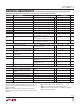
SYMBOL PARAMETER CONDITIONS MIN TYP MAX UNITS
V
THR_ENABLE
ENABLE Threshold 0.8 1.4 2 V
I
ENABLE
ENABLE Input Current ENABLE from 0V to V
CC
●
0.1 ±5 μA
t
PLH_EN
ENABLE Delay Off-On V
CC
= 3.3V (Figure 1) 95 μs
t
PHL_EN
ENABLE Delay On-Off V
CC
= 3.3V (Note 3) (Figure 1) 10 ns
t
PLH_READY
READY Delay Off-On V
CC
= 3.3V (Note 3) (Figure 1) 10 ns
t
PHL_READY
READY Delay On-Off V
CC
= 3.3V (Note 3) (Figure 1) 10 ns
V
OL_READY
READY Output Low Voltage I
PULLUP
= 3mA, V
CC
= 2.3V
●
0.4 V
I
OFF_READY
READY Off Leakage Current V
CC
= READY = 5.5V
●
0.1 ±5 μA
Propagation Delay
t
PHL
SDA/SCL Propagation Delay High to Low C
LOAD
= 50pF, 2.7k to V
CC
on SDA, SCL,
V
CC
= 3.3V (Notes 2, 3) (Figure 1)
70 ns
t
PLH
SDA/SCL Propagation Delay Low to High C
LOAD
= 50pF, 2.7k to V
CC
on SDA, SCL,
V
CC
= 3.3V (Notes 2, 3) (Figure 1)
10 ns
t
FALL
SDA/SCL Transition Time High to Low C
LOAD
= 100pF, 10k to V
CC
on SDA, SCL,
V
CC
= 3.3V (Notes 3, 4) (Figure 1)
30 300 ns
Input-Output Connection
V
OS
Input-Output Offset Voltage 2.7k to V
CC
on SDA, SCL, V
CC
= 3.3V,
Driven SDA, SCL = 0.2V
●
20 60 100 mV
V
THR
SDA, SCL Logic Input Threshold Voltage Rising Edge 0.45V
CC
0.55V
CC
0.65V
CC
V
V
HYS
SDA, SCL Logic Input Threshold Voltage
Hysteresis
(Note 3) 50 mV
C
IN
Digital Input Capacitance SDAIN, SDAOUT,
SCLIN, SCLOUT
(Note 3) 10 pF
I
LEAK
Input Leakage Current SDA, SCL, Pins
●
±5 μA
V
OL
Output Low Voltage SDA, SCL Pins, I
SINK
= 4mA,
SDAIN/SCLIN = 0.2V, V
CC
= 2.7V
●
0 0.4 V
2.7k to V
CC
on SDA, SCL, V
CC
= 3.3V,
Driven SDA, SCL = 0.1V
●
120 160 205 mV
V
ILMAX
Buffer Input Logic Low Voltage V
CC
= 3.3V
●
1.2 V
Timing Characteristics
f
I2C,MAX
I
2
C Maximum Operating Frequency (Note 3) 400 600 kHz
t
BUF
Bus Free Time Between Stop and Start
Condition
(Note 3) 1.3 μs
t
HD,STA
Hold Time After (Repeated) Start Condition (Note 3) 100 ns
t
SU,STA
Repeated Start Condition Set-Up Time (Note 3) 0 ns
t
SU,STO
Stop Condition Set-Up Time (Note 3) 0 ns
t
HD,DATI
Data Hold Time Input (Note 3) 0 ns
t
SU,DAT
Data Set-Up Time (Note 3) 100 ns
The ● denotes the specifi cations which apply over the full operating
temperature range, otherwise specifi cations are at T
A
= 25°C. V
CC
= 3.3V, unless otherwise noted.
ELECTRICAL CHARACTERISTICS
Note 1: Stresses beyond those listed under Absolute Maximum Ratings
may cause permanent damage to the device. Exposure to any Absolute
Maximum Rating condition for extended periods may affect device
reliability and lifetime.
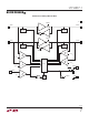
Note 2: See “Propagation Delays” in the Operations section for a
discussion of t
PHL
and t
PLH
as a function of pull-up resistance and bus
capacitance.
Note 3: Determined by design, not tested in production.
Note 4: Measure points are 0.3 • V
CC
and 0.7 • V
CC
.
Note 5: I
CC
test performed with connection circuitry active.
Note 6: All currents into pins are positive; all voltages are referenced to
GND unless otherwise specifi ed.