
Datasheet

LTC4307-1
6
43071fa
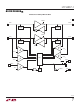
PI FU CTIO S
UUU
ENABLE (Pin 1): Connection Enable Input. This is a 1.4V
digital threshold input pin. For normal operation pull or tie
ENABLE high. Driving ENABLE below 0.8V isolates SDAIN
from SDAOUT, SCLIN from SCLOUT and asserts READY
low. A rising edge on ENABLE after a fault has occurred
forces a connection between SDAIN, SDAOUT and SCLIN,
SCLOUT. Connect to V
CC
if unused.
SCLOUT (Pin 2): Serial Clock Output. Connect this pin to
the clock line of a DDC bus. A pull-up resistor should be
connected between this pin and a supply voltage greater
than or equal to the V
CC
voltage.
SCLIN (Pin 3): Serial Clock Input. Connect this pin to
the clock line of a DDC bus. A pull-up resistor should be
connected between this pin and a supply voltage greater
than or equal to the V
CC
voltage.
GND (Pin 4): Device Ground. Connect this pin to a ground
plane for best results.
READY (Pin 5): Connection READY Status Output. The
READY pin is an open-drain N-channel MOSFET output that
pulls low when ENABLE is low, or when the start-up and
connection sequence described in the Operation section
has not been completed. READY goes high when ENABLE
is high and a connection is made. READY can be used to
control the HDMI HPD signal. Connect a pull-up resistor,
typically 10k, from this pin to V
CC
to provide the pull-up.
This pin can be fl oated if unused.
SDAIN (Pin 6): Serial Data Input. Connect this pin to the
data line of a DDC bus. A pull-up resistor should be con-
nected between this pin and a supply voltage greater than
or equal to the V
CC
voltage.
SDAOUT (Pin 7): Serial Data Output. Connect this pin to
the data line of a DDC bus. A pull-up resistor should be
connected between this pin and a supply voltage greater
than or equal to the V
CC
voltage.
V
CC
(Pin 8): Supply Voltage Input. Place a bypass capacitor
of at least 0.01μF close to V
CC
for best results.
Exposed Pad (Pin 9, DFN Package Only): Exposed Pad
may be left open or connected to device ground.